Meet FAMES at ESSERC 2026 in Mallorca
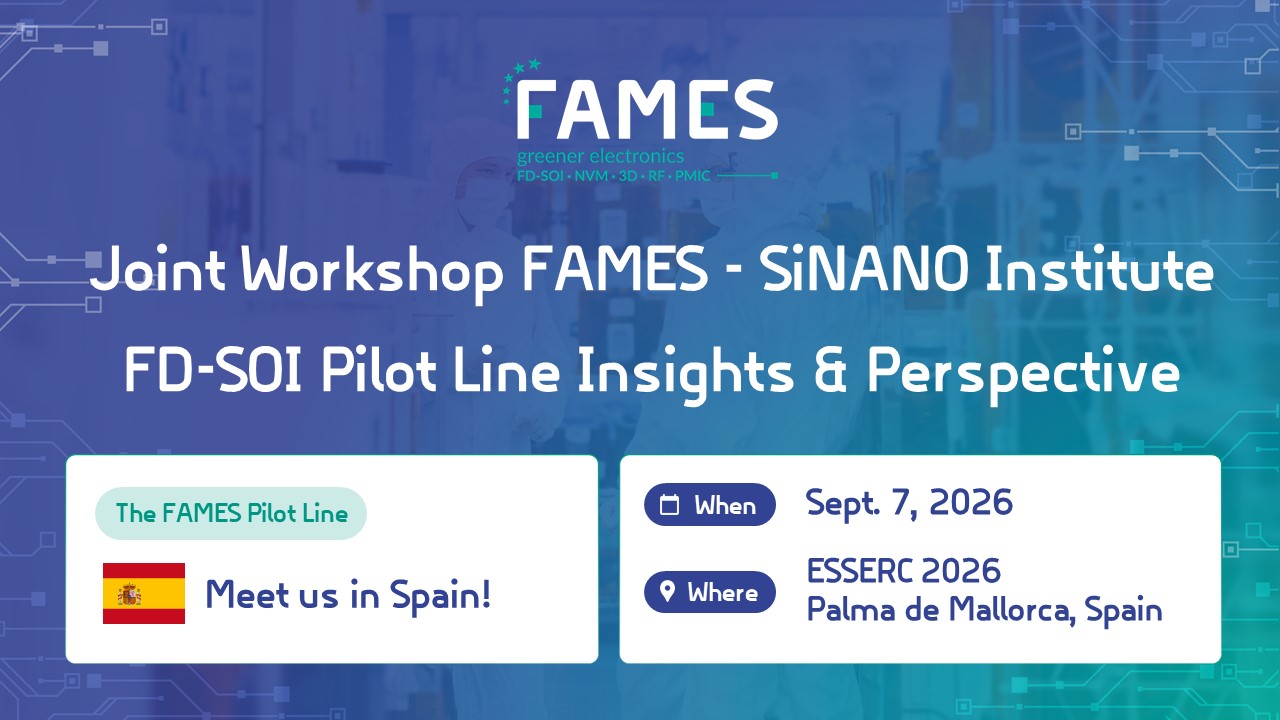
The FAMES Pilot Line will participate in ESSERC 2026, taking place from 7 to 10 September 2026 in Palma de Mallorca, Spain.
Recognised as one of Europe’s leading conferences on solid-state devices and circuits, ESSERC brings together researchers, technologists, device experts, IC designers and system architects to discuss the latest advances shaping the future of semiconductor technologies.
FAMES Workshop – 7 September
On 7 September, FAMES and the SiNANO Institute will host a dedicated half-day workshop entitled: “FDSOI Pilot Line Insights and Perspective”
This session will be the first opportunity to present in-depth technical results from the FAMES Pilot Line on the development of 10 nm and 7 nm FD-SOI technologies.
Programme
FAMES and SiNANO Introductions
14:00 – 14:15
Dominique Noguet, CEA-Leti FAMES Coordinator
Abstract “The FAMES pilot line, opportunities for next generation of chips”: FAMES is one of the five Pilot Lines launched by the Chips JU as part of the Chips Act 1 to support European sovereignty in the area of micro and nano electronics. Five technologies are being developed in the framework of this ambitious 830M€ initiative: FD-SOI, eNVM, RF passive components, 3D integration and power management IC, along with an eco-innovation program. This interlocutory talk will give an overview of the activities of FAMES and will stress how the semiconductor ecosystem can gain access to the technologies and the Pilot Line of the project.
Dominique Noguet
Dominique Noguet is the coordinator of the FAMES Pilot Line, and VP at CEA-Leti. Prior to this role he held several positions as digital IC designer, lab manager and department manager. He led many projects at a national level and in European frameworks (FP5, FP6, FP7), and large industrial partnerships. Dominique has authored or co-authored 100+ scientific papers (several best paper awards), several book chapters and 15 patents. He was a reviewer and a member of scientific committees of international conferences and a member of journal editorial boards. He was conference chair and TPC chair of several international conferences, and is an IEEE Senior Member. Dominique holds an engineering degree of the National Institute of Applied Sciences (INSA) in electrical engineering in 1992, and a PhD from National Polytechnical Institute of Grenoble (INPG) in 1998.

Giorgos Fagas, SiNANO Institute’s Director
Giorgos fagas
TBC
Next generations of FD-SOI technology for low-power and RF applications
14:15 – 14:40
Thierry Poiroux – CEA-Leti
Abstract: In this presentation, we will first detail the 10 nm FD-SOI technology developed in the FAMES pilot line, emphasizing performance boosters to meet specifications. The second part will discuss FD-SOI transistor specificities and their exploitation at the circuit level. We will explore how these unique characteristics can be leveraged to enhance circuit performance and efficiency. The presentation aims to provide insights into the technological advancements and practical applications of FD-SOI technology.
Thierry Poiroux
Thierry Poiroux received the M.S. degree from Ecole Centrale Paris, France, in 1995 and the Ph.D. degree from the University of Nantes, France, in 2000. After a Ph.D. work carried out at the Commissariat à l’Énergie Atomique/Laboratoire d’Electronique et de Technologie de l’Information (CEA–Leti), Grenoble, France, and Matra MHS on plasma process-induced damage, he joined CEA–Leti as a Research Staff Member in 2000. Until 2002, he was involved in partially and fully depleted silicon-on-insulator (SOI) process integration and compact modeling. From 2002 to 2010, he worked on advanced device architectures and was in charge of multiple-gate device modeling, planar double gate process integration and fabrication of graphene-based transistors. In 2011 and 2012, he has been the Head of the Innovative Device Laboratory of CEA–Leti, dedicated to the development of advanced CMOS technologies. From 2012 to 2018, he developed the second version of the L–UTSOI compact model, selected by the Si2 Compact Model Coalition as a standard industrial model for fully-depleted SOI technologies. From 2018 to 2021, he was the head of the Simulation and Compact Model Laboratory of CEA–Leti. From 2021 to March 2025, he was in charge of the Characterization, Design and Simulation Department, and he is currently project leader. He has authored or coauthored five book chapters and about 190 papers and communications, and he is author or co-author of about 20 patents.

What achievements FAMES already produced for the development of Embedded Non Volatile Memories in Europe
14:40 – 15:05
Gabriel Pares – CEA-Leti
Abstract: Emerging eNVM are essential add-on technologies for FD-SOI platforms at the 10 and 7 nm nodes where flash will no longer be working. In FAMES pilot line we are developing four main flavors of eNVM (OxRAM, FeRAM, MRAM and BEOL Fe(M)FET), each of which having significant advantages for addressing specific applications targeted for FD-SOI, particularly for artificial intelligence and security. This presentation will give an overview of the status we have reached and the progresses made at the midterm of FAMES timeline.
Gabriel Parès
Gabriel Parès has an Engineer degree in “material science” from l’Institut National des Sciences Appliquées (INSA) de Lyon, France and a postgraduate degree in “semiconductor material sciences” from the University of Lyon.
He has been working for 33 years in semiconductors and MEMS industry in industrial and R&D fields, formerly for STMicroelectronics and MEMScap, then he joined CEA-leti in 2004.
He has been working from 2010 to 2020 in the field of 3D integration and advanced packaging technologies. Since 2021 he is project manager in the Laboratory of Memories and Computing in charge of the work package dedicated to embedded Non Volatile memories of the FAMES pilot line. He holds 18 patents and he is the author of 19 publications in different fields of semiconductors technologies.

2D Materials on FD-SOI: Enabling New Functionalities Beyond Moore
15:05 – 15:30
Francisco Gamiz – University of Granada
Abstract: This talk will present the role of two-dimensional materials and FD-SOI technologies in enabling More-than-Moore applications within the FAMES Pilot Line. As CMOS scaling increasingly requires heterogeneous integration, 2D materials such as graphene and transition metal dichalcogenides offer unique opportunities for sensing, optoelectronics, memory, and neuromorphic functions directly integrated with advanced silicon platforms. The presentation will discuss how FD-SOI provides an excellent technological base for low-power, highly sensitive, and reconfigurable systems, while 2D materials add new device functionalities beyond conventional logic. Special attention will be given to wafer-scale growth, BEOL-compatible processing, clean-room integration, and the challenges associated with contacts, variability, reliability, and process contamination. The contribution of the University of Granada within FAMES will be highlighted, focusing on the development of transfer-free 2D material integration routes and their potential impact on future European semiconductor pilot lines and application-driven technology demonstrators.
Francisco Gamiz
Francisco Gamiz is Professor of Electronics and Computer Science at the University of Granada and Director of CITIC-UGR. He leads the Nanoelectronics, Graphene and Two-Dimensional Materials Laboratory, where his research focuses on advanced nanoelectronic devices, FD-SOI technologies, 2D materials, biosensors, memristive memories, and semiconductor process integration. He has coordinated and participated in national and European projects, collaborating with academic and industrial partners in microelectronics, sensing, and emerging device technologies. He is also actively involved in scientific leadership, conference organization, and technology-transfer initiatives, contributing to the development of next-generation semiconductor platforms and clean-room capabilities at UGR and beyond internationally.

Coffee Break
15:30 – 15:50
Solidly Mounted Lithium Niobate Bulk Acoustic Wave Filters for the FR3 range
15:50 – 16:15
Alexandre Reinhardt – CEA-Leti
Crowding of the sub-6 GHz wireless spectrum and the need for increasing data rates have pushed 5G to exploit mmWave frequencies. However, this limits data transfer to short distance and line-of-sight links. In view of this, 6G proposes to exploit the FR3 range (7-24 GHz), which seems a promising compromise. Mobile communication will however have to share the spectrum with already existing satellite or emergency services. This requires suitable bandpass filters. In this talk, we present on-going work at CEA Leti towards bringing acoustic filters from the sub-6 GHz to the FR3 range by leveraging the use of single crystal piezoelectric materials.
Alexandre Reinhardt
Alexandre Reinhardt is a senior technical expert with 25 years of experience in developing acoustic wave resonators and filters for the wireless communication industry. After a PhD at the FEMTO-ST Institute (Besançon, France) sponsored by Temex (now Qualcomm France), he joined CEA-Leti in 2006. His research focuses particularly on bulk acoustic wave resonators, their modeling and the design of these devices, to answer the need to continuously increase operation frequencies and quality factors. In the past decade, he has particularly investigated the use of single crystal highly piezoelectric materials such as lithium niobate, which now find applications in the filtering industry.

Advancing 3D Sequential Integration: Process Innovations and Future Applications
16:15 – 16:40
Perrine Batude – CEA-Leti
Abstract: 3D Sequential Integration (3DSI) enables the stacking of diverse device layers with unparalleled contact density thanks to lithographic alignment.
The FAMES project aims to expand the applicability of 3DSI to “More than Moore” applications, targeting advanced imaging systems, energy-efficient computing, and RF circuits.
This presentation will provide key process elements for realizing components in 3D sequential integration and offer a vision of the targeted applications for the future.
We summarize our latest advancements, including the development of versatile 2.5V n & p SOI MOSFETs fabricated entirely at 400°C, overcoming critical low-temperature challenges and enabling large-scale industrial adoption. Additionally, we demonstrate the first radio-frequency circuits fabricated in the top-tier of a full 3D Sequential Integration process at mmW for 5G applications, showcasing the feasibility of vertical co-integration without degradation despite the close vicinity of both tiers.
Perrine Batude
Perrine Batude obtained her Ph.D. from the Institut National Polytechnique de Grenoble in 2009, where she began her work on 3D Sequential Integration (3DSI) at CEA-Leti. She has been instrumental in developing this technology at Leti for over 15 years, with a focus on semiconductor devices, particularly FDSOI transistors, low-temperature processes, and direct bonding techniques. Her work has contributed to advancing 3DSI for various applications including computing, imaging, and RF systems. She has published over 150 papers in scientific journals and conference proceedings, and holds more than 30 patents in semiconductor technology. Currently, she leads the 3D Sequential Integration work package in the FAMES project.

The Rise of Heterogeneous Integration and 3D architectures as key enablers in the AI era.
16:40 – 17:05
Emmanuel Ollier – CEA-Leti
Abstract: The push toward sub-2nm transistor nodes and innovative device architectures is essential to meet the performance demands in the AI era. Yet, this alone is no longer sufficient. The soaring computational needs of cloud servers and edge-AI call for groundbreaking architectures that drastically cut data movement, latency, and power consumption.
These new architectures are made possible by major advances in advanced packaging and heterogeneous integration, technologies that have become pivotal in semiconductor ecosystems.
This presentation will demonstrate how the FAMES Pilot Line drives innovation in advanced packaging, notably through small-pitch hybrid bonding and through-silicon via (TSV) technologies. It will also showcase how these technologies enable novel architecture designs for computing and RF systems.
Emmanuel Ollier
Dr. Emmanuel Ollier is the EU Program Manager at CEA-Leti’s Semiconductor Components Division. Previously, he led the Laboratory of 3D Integration and Advanced Packaging Technologies at CEA-Leti. With 17 years of experience in the semiconductor industry (including roles at Thales, Atmel, NXP, EM Microelectronics) he holds 22 patents and has authored 45 papers and international conference presentations. Dr. Ollier earned a PhD in Material Sciences and an Engineering Degree from the French National School of Physics and Chemistry of Bordeaux. His expertise focuses on the heterogeneous integration of semiconductor and photonic technologies, with applications spanning High-Performance Computing, Edge-AI, RF communications, smart sensors and displays, and power electronics.

Small inductors for DC-DC converters: Power Management Integrated Circuits.
17:05 – 17:30
Sambuddha Khan – Tyndall National Institute
Abstract: High-frequency on-chip power supplies demand inductors co-located with power management ICs, yet monolithic BEOL integration of magnetics is constrained by thermal budget and thin metallisation. This talk presents Tyndall’s magnetics-on-silicon platform and the heterogeneous integration solution developed within the FAMES Pilot Line: model-based design of stripline micro-inductors (5–10 nH, 20–50 MHz) for multi-level buck converters, optimised CoZrTa/AlN laminated cores, and wafer-level fabrication with quality factors above 8. A tether-free micro-transfer-printing process integrates large-footprint inductor chiplets onto glass substrates and into silicon trenches, preserving inductance within ±10%. Prospects for buried inductor–capacitor power networks in interposers and FAMES access will be discussed.
Sambuddha Khan
Dr Sambuddha Khan is a Senior Scientist and Technical Lead at Tyndall National Institute, Ireland, where his research focuses on the design, fabrication, and heterogeneous integration of MEMS and micro-components, including integrated magnetics, piezoelectric transformers, and AlScN-based RF acoustic resonators for power-supply-on-chip applications. He serves as Programme Manager for Tyndall’s participation in the Chips JU FAMES Pilot Line project and has led research programmes funded by Horizon Europe, Research Ireland, and Enterprise Ireland. Before joining Tyndall, he was a postdoctoral researcher at the University of California, Irvine, working on a DARPA-funded programme on inertial-grade silicon MEMS gyroscopes. Dr Khan received his PhD from the Indian Institute of Science, Bengaluru, in 2014, and lectures at University College Cork on MEMS and microfabrication.

Visit the FAMES Booth
Throughout the conference, attendees will also be able to meet the FAMES team at the project booth.
The booth will provide an opportunity to learn more about:
- FAMES Pilot Line technologies
- Open Access opportunities
- FAMES Academy training activities
- Collaboration opportunities with project partners
Whether you are a researcher, engineer, startup, SME or industrial stakeholder, we invite you to stop by and discuss your projects and innovation needs with our team.
