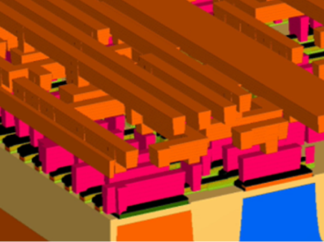
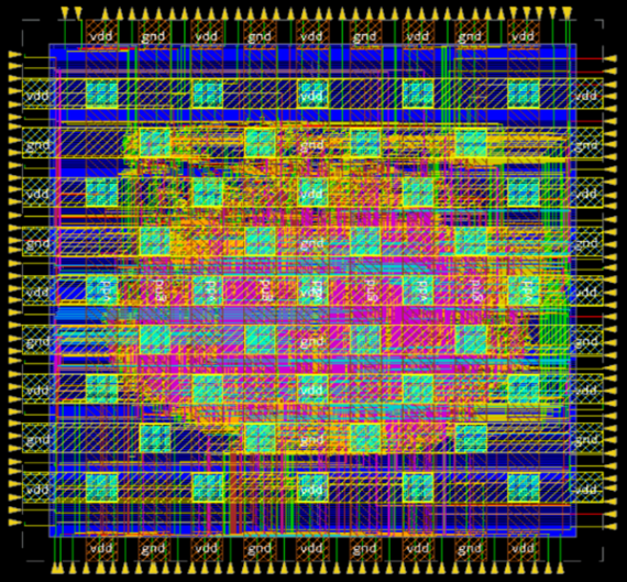
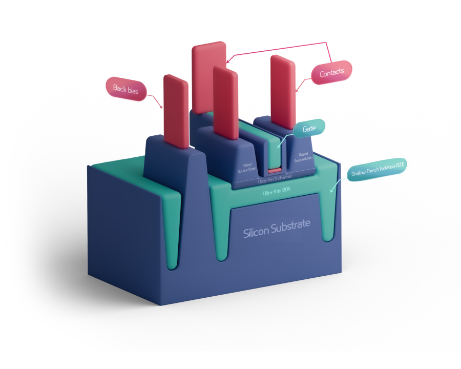
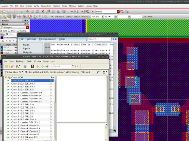
FD-SOI 10nm Pathfinding PDK


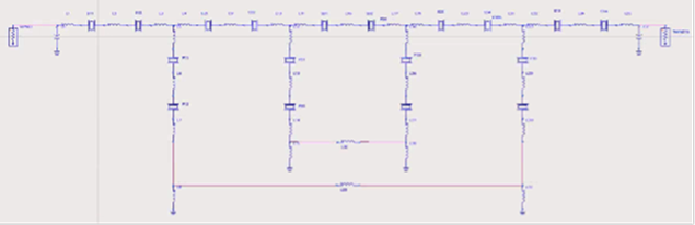
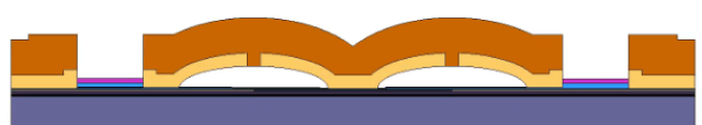
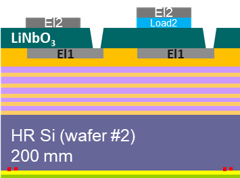
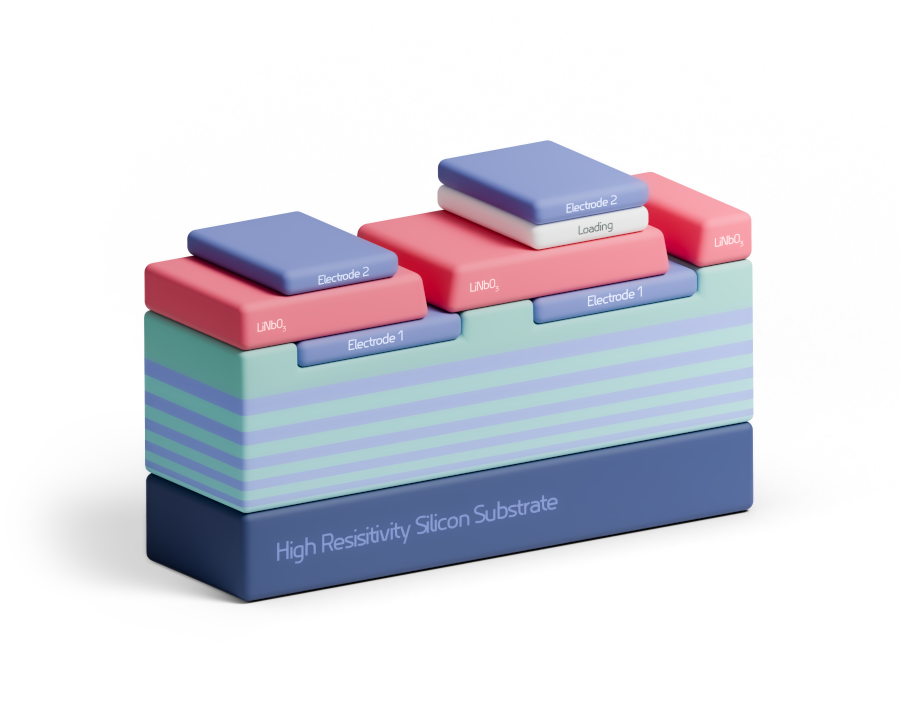
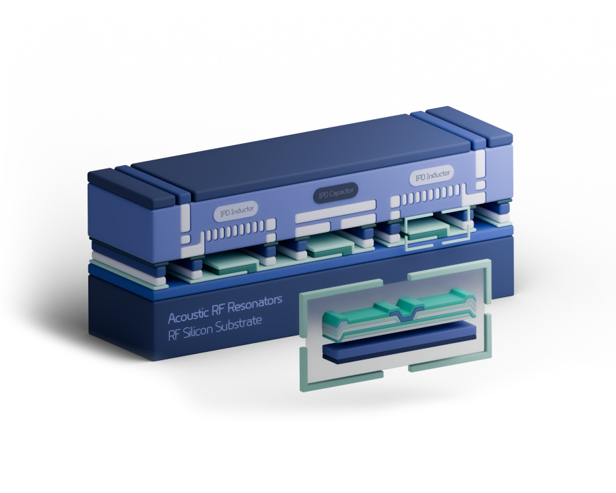
15 GHz LiNbO3 BAW filters
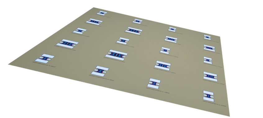
7-15 GHz AlN/ScAlN RF filters
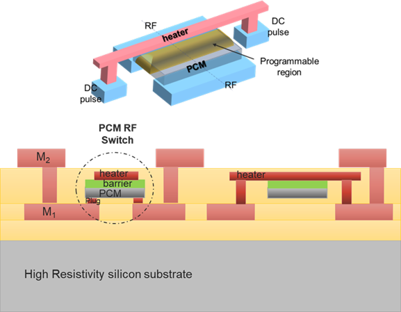
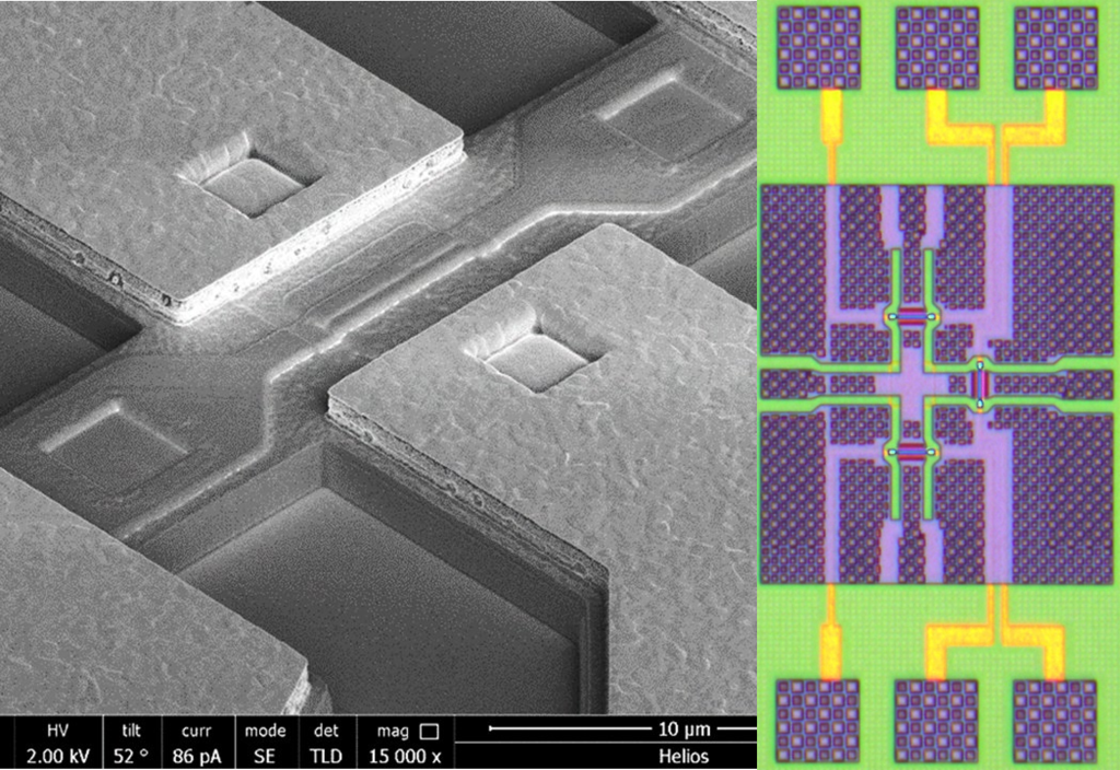
PCM RF switch demonstrators

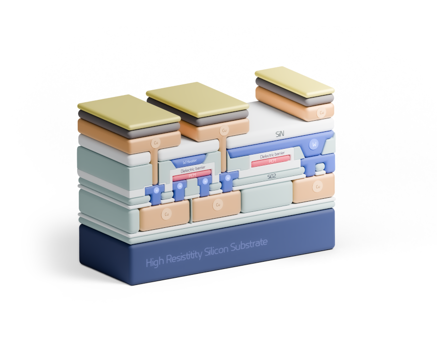
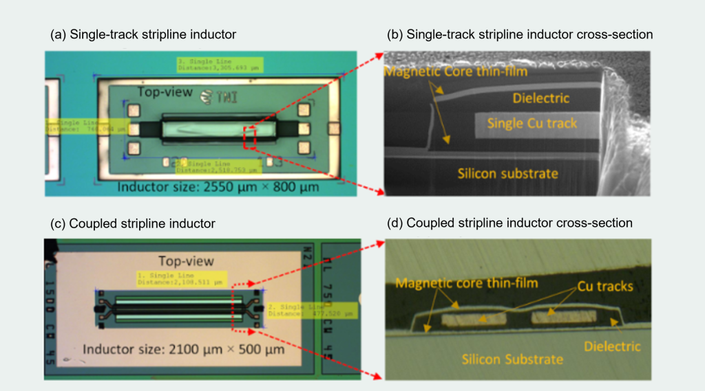
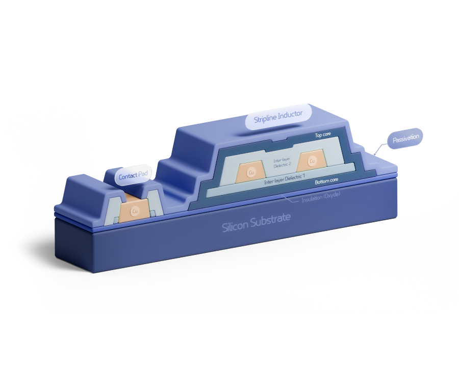
PMIC options: Magnetics on Silicon
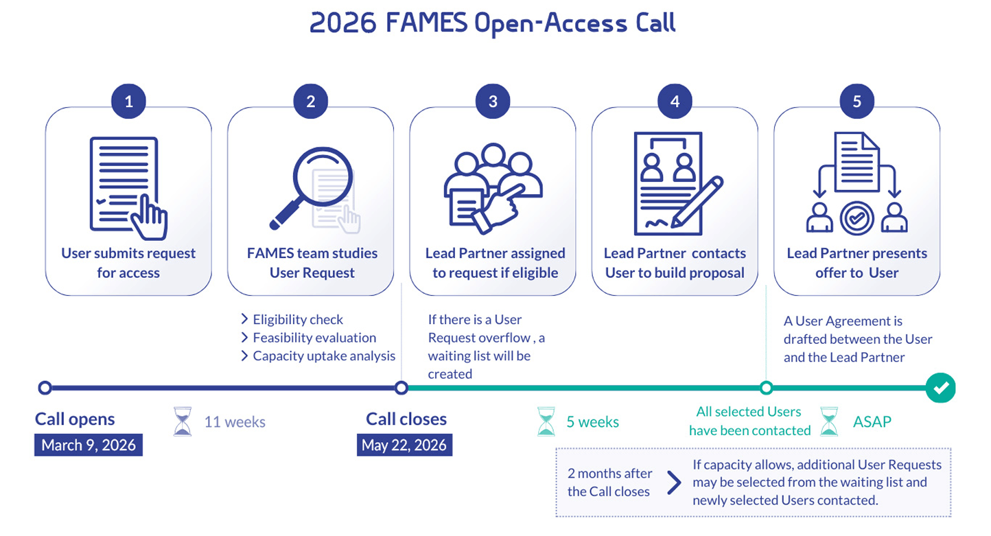
Eligibility refers to the regulations of the European Commission and the participating States concerning the contribution of companies and research institutions to the European semiconductor ecosystem. The Eligibility criteria are listed in Section 5 of the User Guidelines and Procedures.
Please consult the FAMES User Request timeline.
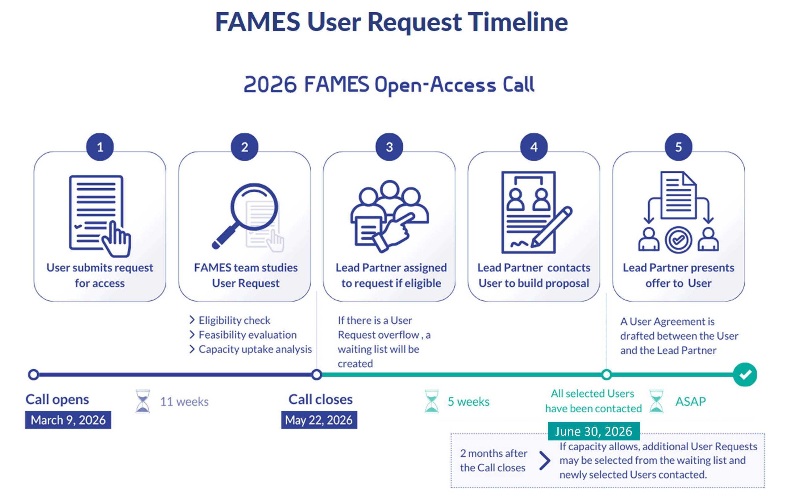
In the event of a User Request overflow, some User Requests will be put on a waiting list. Two months after the submission deadline of the FAMES-Open-Access Call, the waiting list will be reviewed by the Open Access Committee and new User Requests may be selected if the Pilot Line capacity allows it. At this point, Users will be notified of the status of their Request. If their Request cannot be accepted this time around, and depending on the technology requested, it may be possible to resubmit a Request during the following FAMES-Open-Access Call.
FAMES Open-Access Calls will take place every year from 2025 to 2028. They will open in March and close in May.
The PDK is accessible for free but requires signing an NDA and a Design Kit License Agreement (DKLA).
The Open Access Chairperson will be glad to answer any questions you may have regarding the submission form and the FAMES technologies.
