NEWS & RESULTS
News and highlights
- Training
- Equipment
- Technology
FAMES Newsletter
Subscribe to our newsletter to keep up to date with the latest news and achievements of the FAMES project.
The newsletter is released every trimester.
FAMES publications
Articles in Journal
O. Kaatranen, P. Eskelinen, S. Inkinen, O.-P. Kilpi, and K.-M. Persson, Ferroelectric HfO2/ZrO2 Superlattice Capacitors With High Center to Edge Wafer-Scale Uniformity. Advanced Electronic Materials 12, no. 10 (2026): e00773. Open-access version available on https://doi.org/10.1002/aelm.202500773
Iftakher, M.A., Levices, H., Harabi, KE. et al. Intrinsic annealing in a hybrid memristor-magnetic tunnel junction Ising machine. Nat Commun 17, 5246 (2026). Open-access version available on https://doi.org/10.1038/s41467-026-71844-8
Ber K., Wiśniewski P., Modeling of RRAM based PUF: a case study, Solid-State Electronics, DOI: https://doi.org/10.1016/j.sse.2025.109267
Wiśniewski P., Jeżak P., Małkowski A., Kądziela A., Krzemiński J., Mroczyński R., Investigation of compliance current effect on resistive switching properties in Ag/SiOx/Cr RRAM devices, Solid-State Electronics, DOI: https://doi.org/10.1016/j.sse.2025.109288
Merlin, M., Cabaret, T., Grampeix, H., Gauthier, N., Ghostine, M., Kanyandekwe, J., … & Gergaud, P. (2026). Exploring the relationship between doping and Ti-silicidation for advanced FDSOI applications. Microelectronic Engineering, 306, 112482. https://doi.org/10.1016/j.mee.2026.112482
Publications in Conference proceeding/workshop
L. D. Mohgouk Zouknak et al., Strain Engineering for Next-Generation FDSOI MOSFET, Probing CESL Relaxation with Xe, Ar, and Ge Ion Implantation, 2026 International VLSI Symposium on Technology, Systems and Applications (VLSI TSA), HsinChu, Taiwan, 2026, pp. 1-2, doi: 10.1109/VLSITSA69131.2026.11527593.
M. Y. Aliouat, J. Dubois, P. Pimenta-Barros, et al. Plasma etching process tailoring for different polysilicon microstructures used in 10nm FD-SOI metal gate stacks, Proc. SPIE 13984, Advanced Etch Technology and Process Integration for Nanopatterning XV, 1398403 (9 Apr 2026); https://doi.org/10.1117/12.3090459
T. M. Frutuoso et al., Spacer Trapping Effect on Hot Carriers Degradation Dynamics for Advanced FDSOI Nodes, 2026 IEEE International Reliability Physics Symposium (IRPS), Tucson, AZ, USA, 2026, pp. 1-7, doi: 10.1109/IRPS61424.2026.11499220.
M. Najem et al., Die-To-Wafer Hybrid Bonding Technology down to 1 μm pitch for Multi-Die Stacking Integration, 2026 IEEE 76th Electronic Components and Technology Conference (ECTC), Orlando, FL, USA, 2026, pp. 1323-1330, doi: 10.1109/ECTC51846.2026.00218.
M. Faure et al., Hybrid bonding with ultra-low temperature annealing: morphological and electrical validations, 2026 IEEE 76th Electronic Components and Technology Conference (ECTC), Orlando, FL, USA, 2026, pp. 85-90, doi: 10.1109/ECTC51846.2026.00022.
A. Tanwar et al., Tether-Free Micro-Transfer-Printing of Si-based Micro-Inductors: Demonstration of on-Glass and in-Silicon Integration for PowerSoC applications, 2026 IEEE 76th Electronic Components and Technology Conference (ECTC), Orlando, FL, USA, 2026, pp. 1214-1220, doi: 10.1109/ECTC51846.2026.00202.
N. Giovannelli et al., Evaluation of Sidewalls Properties in HZO-Based 3D Ferroelectric Capacitors, 2026 IEEE International Memory Workshop (IMW), Leuven, Belgium, 2026, pp. 1-4, doi: 10.1109/IMW68301.2026.11532893.
H. Levices et al., In-depth energy analysis of a hybrid sMTJ/RRAM Ising machine, 2026 International VLSI Symposium on Technology, Systems and Applications (VLSI TSA), HsinChu, Taiwan, 2026, pp. 1-2, doi: 10.1109/VLSITSA69131.2026.11527654.
Articles in Journal
Martínez A., Márquez C., Lorenzo F., Gutiérrez F., Caño-García M., Ávila J., Carlos Galdón Gil J., Ortega Lopez R., Navarro C., Donetti L., Gámiz F., Wafer-Scale Demonstration of BEOL-Compatible Ambipolar MoS2 Devices Enabled by Plasma-Enhanced Atomic Layer Deposition, ACS Applied Materials & Interfaces, DOI: 10.1021/acsami.5c12014
Tran, N. P., Tran, N., Milesi, F., Le, V. H., Zouknak, L. D., Dezest, P., … & Fenouillet-Beranger, C. Toward Full Relaxation of Ssoi Substrates for Pfet Device Fabrication. P. and Rodriguez, Philippe and Brunet, Laurent and Duriez, B. and Cyrille, MC. and Fenouillet-Beranger, C., Toward Full Relaxation of Ssoi Substrates for Pfet Device Fabrication. doi: 10.1016/j.sse.2025.109196
Zouknak, L. M., Le, V. H., Tran, N. P., Milesi, F., Hartmann, J. M., Jarjayes, S., … & Fenouillet-Beranger, C. (2025). Nanoscale SOI strain engineering: STRASS-enabled local stress optimization. Solid-State Electronics, 109215. doi: 10.1016/j.sse.2025.109215
Bazzi, A., Levices, H., Talatchian, P., Badets, F., & Hutin, L. (2025). Ising-inspired invertible adders using coupled phase-locked CMOS ring oscillators. Physical Review Applied, 24(1), 014004. doi: https://doi.org/10.1103/8xc2-vkk3
Fenouillet-Beranger, C., Rozeau, O., Chouk, R., Cueto, O., Royet, A. S., Charbonneau, M., … & Noguet, D. Pursuing the Fd-Soi Roadmap Down to 10-7nm Nodes for High Energy Efficient, Low Power and Rf/Mmwave Applications. doi: 10.2139/ssrn.5316840
Barge, D., Gallard, M., Hartmann, J. M., Fournel, F., Loup, V., Mazen, F., … & Servant, F. 300 Mm Ssoi Engineering with Ultra Thin Box. Available at SSRN 5316841: doi.org/10.2139/ssrn.5316841 – Open-access version available on HAL: https://cea.hal.science/cea-05265844v1/document
Marquez, C., Gity, F., Galdon, J. C., Martinez, A., Salazar, N., Ansari, L., … & Gamiz, F. (2025). On the Enhanced p‐Type Performance of Back‐Gated WS2 Devices. Advanced Electronic Materials, 2500079. doi: https://doi.org/10.1002/aelm.202500079
Lèquepeys, JR., Noguet, D., Paing, B. et al. Europe’s pilot line on fully depleted silicon-on-insulator technology (FAMES). Nat Rev Electr Eng 2, 77–78 (2025). https://doi.org/10.1038/s44287-025-00144-y
Milesi, F., Rodriguez, P., Zouknakl, L.D.M. et al. Process challenges of the STRASS technique to increase the electron mobility in advanced FD-SOI nMOSFETs. MRS Advances 10, 174–178 (2025). https://doi.org/10.1557/s43580-025-01148-4 – Open-access version available on HAL: https://hal.science/hal-04935690v1/document
Bonnet D., Cottart K., Hirtzlin T., Januel T., Dalgaty T., Vianello E., Querlioz D., Bayesian continual learning and forgetting in neural networks, Nature Communications volume 16, Article number: 9614 (2025), DOI: https://doi.org/10.1038/s41467-025-64601-w – Open-access version available on HAL: https://cnrs.hal.science/hal-05358004v1/document
Publications in Conference proceeding/workshop
Fidon, E.; Guillou, S.; Rivoira, Y.; Vauche, L. Electronic-Grade Silicon (EG Si) Wafer Production: Review and Update of Life Cycle Inventory (LCI) Data. Eng. Proc. 2026, 127, 16. Open-access version available on https://doi.org/10.3390/engproc2026127016
Bosch D. , Vandendaele W., Diallo E-A., Royet A-S., Albouy A., Opprecht M., Darras F-X., Benevent V., Maillard P., Adami O., Ribotta M., Kerdilès S., Gassilloud R., Garros x. and Batude P., High Performance 2.5V n&p 400°C SOI MOSFETs: a Breakthrough for versatile 3D Sequential Integration, IEDM. doi: 10.1109/IEDM50572.2025.11353514.
Lehninger D., Zhang T., Reinig P., Barbot J., Opprecht M., Kerdiles S., Grenouillet L., Seidel K., Lederer M., Enhanced Ferroelectricity in Hf0.5Zr0.5O2 Thin Films by NLA at Intermediate Laser Energy Density, 2025 International Conference on IC Design and Technology (ICICDT), Lecce, Italy, 2025, pp. 61-64. doi: 10.1109/ICICDT65192.2025.11078051
Szekrényes, Z., Le, V. H., Bellanger, P., Badeeb, L., Éles, B., Faragó, A. I., … & Laurent, N. (2025, May). In-line Raman spectroscopy for semiconductors strain engineering and control: Topic/Category AM: Advanced Metrology. In 2025 36th Annual SEMI Advanced Semiconductor Manufacturing Conference (ASMC) (pp. 1-4). IEEE. doi: 10.1109/ASMC64512.2025.11010779
Frutuoso, T. M., Vandendaele, W., Bond, A., Bringuier, F., Lapras, V., Cyrille, M. C., … & Garros, B. D. X. (2025, March). Fast CV MSM Technique for Comprehensive Analysis of Bulk Trapping in Low-K Carbon-Doped Dielectrics. In 2025 IEEE International Reliability Physics Symposium (IRPS) (pp. 1-7). IEEE. doi: 10.1109/IRPS48204.2025.10983765
Persson, K. M., Eskelinen, P., Kaatranen, O., & Kilpi, O. P. (2025, June). ITO Contact Optimization for Enhancement Mode BEOL MOSFETs. In 2025 Device Research Conference (DRC) (pp. i-ii). IEEE. doi: 10.1109/DRC66027.2025.11105747
C. Fenouillet-Beranger et al., Ultra-Thin-Body and Buried Oxide FD-SOI next generation nodes and eNVM technologies for advanced IC design, 2025 IEEE 28th International Symposium on Design and Diagnostics of Electronic Circuits and Systems (DDECS), Lyon, France, 2025, pp. 105-114. doi: 10.1109/DDECS63720.2025.11006678 – Open-access version available on HAL: https://hal.science/hal-05085365v1
Grampeix H., Cabaret T., Lespiaux J., Gergaud P., Gauthier N., Rodriguez P.,, Influence of Dopant and Si:B Cap on Ni(Pt)-Based Silicidation of SiGe:B for Next Generation PMOS FDSOI Devices, https://ieeexplore.ieee.org/document/11072894
Zarudniev M., Ouvry L., MassonG., Paviot A., Dehos C., Courouve P., Dual-Mode Wideband Receiver Operating with Frequency Modulated Impulse Radar Waveform, 2025 IEEE Radar Conference, DOI: 10.1109/RadarConf2559087.2025.11205075
Le, M. P., Anthony, C., Michael, P., El, B. S., Julia, S., Bertrand, G., … & Pierre, V. (2025, December). Towards 3D Integration of GaN-on-Si MicroLED and MicroPD Arrays with an Energy-Efficient 22nm FDSOI Transceiver for Short-Range Parallel Optical Communication. In Proceedings of the International Display Workshops – Open-access version available on: https://pub-files.atlas.jp/fs/public/idw2025/ver_15/abstract/en/AMD6-04.pdf
Publications in Conference proceeding/workshop
Kanyandekwe, J., Hartmann, J. M., Lespiaux, J., Marion, T., Saidi, L., Lapras, V., … & Glorieux, O. (2024). Selective Epitaxy of Tensile, Highly Doped SiP for Planar NMOS FD-SOI Devices. ECS Transactions, 114(2), 253. doi: 10.1149/11402.0253ecst
Lespiaux, J., Kanyandekwe, J., Marion, T., Saidi, L., Lapras, V., Bond, A., … & Hartmann, J. M. (2024). Selective Epitaxial Growth of SiGe (: B) for Advanced p-Type Fd-SOI. ECS Transactions, 114(2), 271. doi: 10.1149/11402.0271ecst
Boujnah, A., Cueto, O., Jaud, M. A., Martinie, S., Nallet, F., Fenouillet-Beranger, C., & Rozeau, O. (2024, September). DTCO of advanced FDSOI CMOS technology by process emulation. In 2024 International Conference on Simulation of Semiconductor Processes and Devices (SISPAD) (pp. 01-04). IEEE. doi: 10.1109/SISPAD62626.2024.10733323 – Open-access version available on HAL: https://cea.hal.science/cea-05533763v1/document
Royet, A. S., Chouk, R., Cueto, O., Kanyandekwe, J., Lapras, V., Jaud, M. A., … & Rozeau, O. (2024, September). Calibration Insights of Phosphorus Diffusion Model for NMOS FDSOI: Pathway to Advanced Technology Nodes. In 2024 International Conference on Simulation of Semiconductor Processes and Devices (SISPAD) (pp. 1-4). IEEE. doi: 10.1109/SISPAD62626.2024.10733008
Jarjayes, S., Brunet, L., & Rodriguez, P. (2024, April). Analysis of the key parameters of box creep process for advanced FDSOI devices. In 2024 25th International Conference on Thermal, Mechanical and Multi-Physics Simulation and Experiments in Microelectronics and Microsystems (EuroSimE) (pp. 1-4). IEEE. doi: 10.1109/EuroSimE60745.2024.10491442 – Open-access version available on HAL: https://hal.science/cea-04771615v1
Rodriguez-Fano, M., Pedini, J. M., Cadot, S., Grampeix, H., Magis, T., Laulagnet, F., … & Barraud, S. (2024, September). Comparative study of ALD MoS 2 on high-k dielectrics for the fabrication of nanowire FETs. In 2024 IEEE European Solid-State Electronics Research Conference (ESSERC) (pp. 129-132). IEEE. doi: 10.1149/11402.0271ecst
D. Bosch et al., Breakthrough Processes for Si CMOS Devices with BEOL Compatibility for 3D Sequential Integrated more than Moore Analog Applications, 2024 IEEE Symposium on VLSI Technology and Circuits (VLSI Technology and Circuits), Honolulu, HI, USA, 2024, pp. 1-2, doi: 10.1109/VLSITechnologyandCir46783.2024.10631398.
J. Lugo-Alvarez et al., First Radio-Frequency Circuits Fabricated in Top-Tier of a Full 3D Sequential Integration Process at mmW for 5G Applications, 2024 IEEE Symposium on VLSI Technology and Circuits (VLSI Technology and Circuits), Honolulu, HI, USA, 2024, pp. 1-2, doi: 10.1109/VLSITechnologyandCir46783.2024.10631483 – Open-access version available on HAL: https://cea.hal.science/cea-05170325v1/document
Grampeix, H., Cabaret, T., Kanyandekwe, J., Gauthier, N., Gergaud, P., & Rodriguez, P. Silicidation of Next Generation of FD-SOI Devices: Effect of P Doping Level in epitaxial Si: P Films.
Events
- Event

- Event
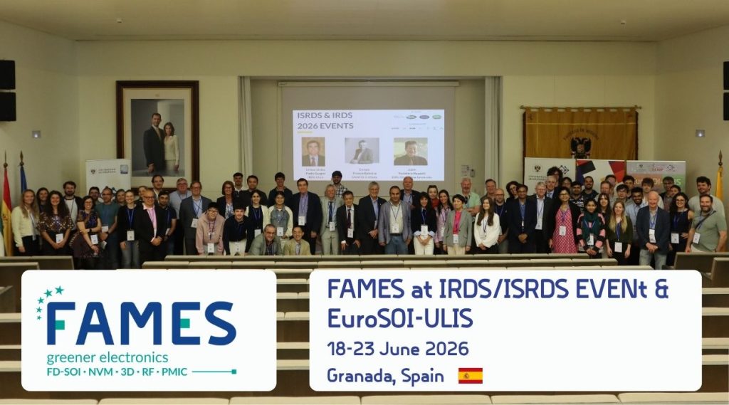
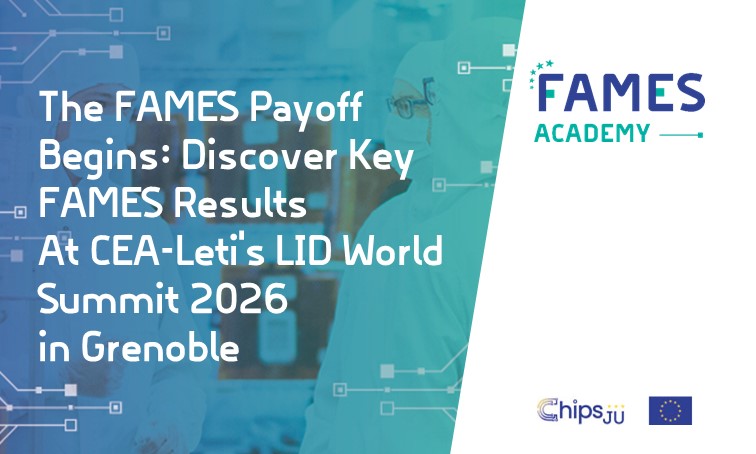
FAMES in Granada: A Week of Scientific Exchange, Innovation and Collaboration From 18 to 22 May 2026, the FAMES Pilot Line team was in Granada, Spain, for a week dedicated...
- Event
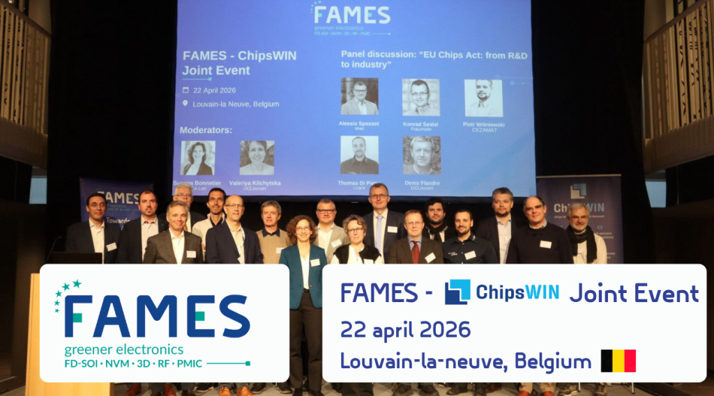
FAMES – ChipsWIN Joint Event The FAMES x ChipsWIN Joint Event, held in Louvain-la-Neuve on the 22 April 2026, gathered around 60 participants from industry, academia, and research organisations. The...
Press releases
- Press Release
- Press Release

- Press Release