NEWS & EVENTS
- Training
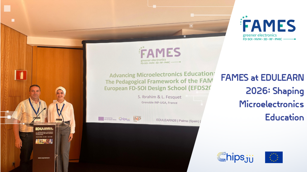
FAMES at EDULEARN 2026: Shaping Microelectronics Education
At EDULEARN 2026, FAMES presented EFDS outcomes, highlighting the European need for hands-on microelectronics training to bridge the skills gap....
- Press Release
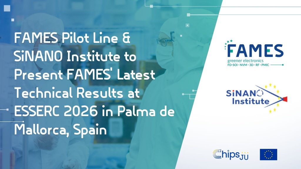
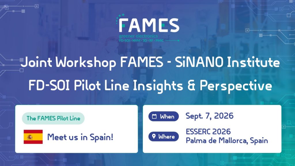
FAMES Pilot Line & SiNANO Institute to Present FAMES’ Latest
The FAMES Pilot Line and SiNANO Institute will host a joint half-day workshop, "FD-SOI Pilot Line Insights and Perspective," on Sept. 7 at ESSERC 2026, the European Solid-State Electronics Research...
- Uncategorized

FAMES at LID World Summit: Where Innovation Meets Collaboration
FAMES at LID World Summit: Where Innovation Meets Collaboration The second FAMES School brought together 190 participants on 24 June 2026 and successfully showcased the opportunities offered by FD-SOI technology....
- Uncategorized
Editorial – FAMES Newsletter #4
Come learn how you, too, can access the FAMES Pilot Line technologies! Join us in Brussels, Belgium on March 18, 2025....
- Uncategorized
Partner’s corner: Christina Hirschl, SAL
Partner’s corner: Christina Hirschl, SAL Silicon Austria Labs (SAL) is Austria’s top research center for electronics and software based systems (ESBS). The application-oriented center offers cooperative research on future-oriented solutions...
- Event
Meet FAMES at ESSERC 2026 in Mallorca
Learn how you can adapt FAMES’ FD-SOI 10-and-7nm process technologies, embedded NVMs, 3D integration, RF components, and power-management IC solutions for your own innovations....
