
FAMES European FD-SOI Design School (EFDS) 2027
- Grenoble, France
- January 25-29, 2027
- pre-registration open
- 1400€ (discount available)*
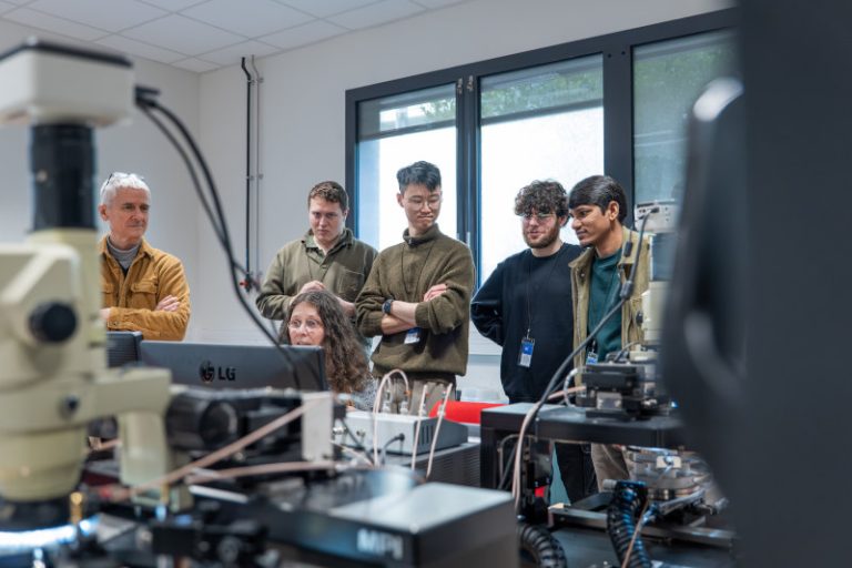
© L.Presumey-CEA
Following the success of the inaugural EFDS session, the 2027 edition will be held at the CIME Nanotech facility in Grenoble from January 25th to 29th.The school addresses the significant scientific and industrial challenges faced by designers, specifically the necessity to balance power, performance, and functionality in modern analog, RF, and digital circuits. FD-SOI technology provides distinct advantages for these requirements, including body-biasing techniques and advanced transistor features that enhance performance, reduce power consumption, and increase design flexibility. The program aims to share the latest industry practices, enabling participants to leverage FD-SOI for the development of more efficient and innovative semiconductor solutions.PrerequisitesThe EFDS is open to:
Registration & Practical InformationThe 1400€ registration fee covers the following:
- PhD candidates and students specializing in microelectronics or semiconductor design.
- Professors and academic researchers seeking to update their knowledge on advanced design flows.
- Industry professionals from European organizations or companies involved in semiconductor technology.
| Monday 25 Jan | Tuesday 26 Jan | Wednesday 27 Jan | Thursday 28 Jan | Friday 29 Jan | |
| 8:30-9:00 AM | Welcome coffee/tea Room A344, CIME Nanotech, 3 Parvis Louis Néel, 38016 Grenoble Cedex 2 | ||||
| 9:00-12 AM | 09:00 – 10:30 AM Welcome Presentation 10:30 – 12:00 AM Presentation to FD-SOI model Room A342 | Course presentation (ACM2 Transistor Model: Parameter extraction and circuit design in FD-SO) Room A342 | G1, G2 & G3 | TP Digital: 1st part (G1, G2 & G3) Rooms A446 – A447 | TP Digital: 2nd part (PNR) (G1, G2 & G3) Rooms A446 – A447 |
| 12:00-14:00 PM | Lunch break | ||||
| 14:00-15:45 PM | Presentation to FD-SOI model Room A342 | Hands-on practical session (G1, G2 & G3) Rooms A446 – A447 | Course presentation (Design of digital circuits in FD-SOI) Room A342 | 14:00 – 16:00 PM TP characterisation (G1) Room Elec. Charac 14:00 – 16:00 PM Layout session in FD-SOI (G2) Room A446 14:00 – 15:30 PM TP RF Circulator (G3) Room RF Platform | Presentation of Pathfinding PDK & open access call Room A342 |
| 15:45-16:00 PM | Coffee/tea break Room A344 | ||||
| 16:00-18:00 PM | 16:00 – 17:30 PM Lecture RF Circulator Room A342 | Hands-on practical session (G1, G2 & G3) Room A446-A447 | 4:30-6:00 PM Site Visit (Soitec) | 16:00 – 18:00 PM TP characterisation (G2) Room Elec. Charac 14:00 – 16:00 PM Layout session in FD-SOI (G3) Room A446 14:00 – 15:30 PM TP RF Circulator (G1) Room RF Platform | |
| 19:00-21:00 PM | Social Dinner | ||||
- Full access to all training modules and practical sessions.
- All breakfast, coffee breaks, and lunches during the five-day event.
- Participation in the scheduled networking dinner and group cohesion activity.
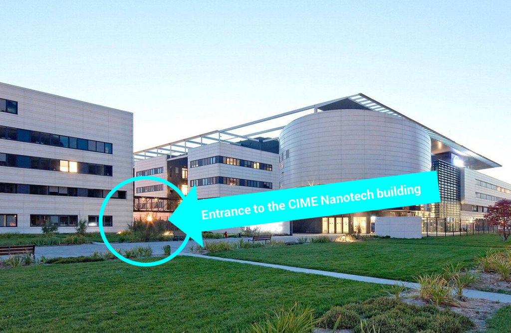
Address and directions
The EFDS is held in the CIME Nanotech building at
3 Parvis Louis Néel – Minatec
38016 Grenoble Cedex 1.
Curious about the last edition of the EFDS ?
Discover the recap video !


