eNVM

Embedded non-volatile memory (eNVM)

Embedded non-volatile memories (eNVM) are small-sized memory circuit embedded in a larger application IC to deliver a full system-on-chip functionality to meet a variety of system applications. Today, it is primarily used in smart cards, SIM cards, microcontrolers and display drivers, to name a few.

Access PDKs giving access to Silicon- Technologies - FAMES Pilot line
Credit: CEA-Leti/S. Martin et al, “Hf0.5Zr0.5O2 FeRAM scalability demonstration at 22nm FDSOI node for embedded applications”, IEDM Symposium 2024

A Non Volatile Memory is a memory able to retain data even when powered off. NVM have been available for a long time, examples being flash and EEPROM memories, but new technologies are emerging such as Resistive Random-Access Memory (ReRAM), Magnetic Random-Access Memory (MRAM), Phase Change Memory (PCM) and Ferroelectric Random-Access Memory (FeRAM), among many others. They have the potential to replace all or most of the existing semiconductor memory technologies as they consume less power and are easily scalable for next generation applications.

Embedding eNVM in the chip back end of line (BEOL) is a recent concept that solves the difficulties of co-integrating memories and CMOS logic in advanced nodes and can dramatically reduce power consumption and opens a path towards new applications. For instance, generalizing the concept of in-memory-computing by natively integrating large NVM arrays make disruptive computing paradigms possible with a goal of improving the energy/power efficiency by orders of magnitude at the application level. Today, different BEOL eNVM flavors exist on FD-SOI but their usage in products is still limited and their scaling has still to be pushed forward.

The FAMES project will develop OxRAM, MRAM, FeFET and FeRAM. These eNVM flavors of are complementary: they address different application requirements.

Magnetic Random Access Memories (MRAM) are composed of a magnetic free layer and a magnetic pinned layer separated by a tunnel barrier. State-of-the-art Spin-Transfer Torque (STT) MRAM uses spin-aligned electrons to directly flip the magnetic domains. This type of memory is well suited for general purpose chips. It may even replace SRAM in the last levels of cache because of its high endurance and high speed.

Oxide-based RAM (OxRAM) consists of a dielectric material (typically HfO2) inserted between two metallic electrodes. Initially at the High Resistance State (HRS), the creation of a filament of oxygen vacancies in the oxide shifts the memory towards the Low-Resistive State (LRS). This phenomenon is stable and reversible, ensuring the retention and endurance of the device. This is a low-end, low-cost memory that is simple to manufacture, well suited for consumer applications.

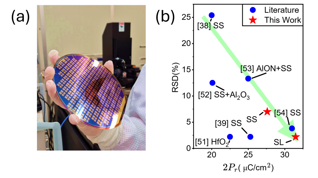
Ferroelectric memories (FeRAM, FeFET) are based on the electrical polarization modulation of a ferroelectric material integrated in a BEOL capacitor. Recent demonstrations of ferroelectric hafnium zirconium oxide (HZO) integrated in the BEOL, translate into a low-cost, highly scalable ferroelectric memory solution. Contrarily to MRAM, OxRAM or PCM, the programming of ferroelectric memories is not current-based but rather driven by the electric field. Some ferroelectric memory devices are thus well adapted for energy-efficient systems, as well as embedded DRAM replacement (high-density, high-speed).

FAMES has the ambition to integrate eNVM devices in the BEOL, as an add-on feature to 10 and 7nm FD-SOI technology nodes, opening opportunities for disruptive chip architectures. FAMES partners will join their expertise to strengthen the FAMES Pilot Line offer by developing a wide range of competitive eNVMs adapted to FD-SOI nodes beyond 22 nm, namely OxRAM, MRAM, FeFET and FeRAM.

In the last 10 years, breakthrough technologies, such as the Internet of Things (IoT), Artificial Intelligence (AI) and 5G have changed our daily lives with smart homes and buildings, industry 4.0, smart mobility, personalized healthcare, precision farming and wearables. This evolution was made possible by the semiconductor industry and the design and fabrication of more complex chips, as well as the integration of larger and larger eNVM capacity. The result is a more cost effective development of smart devices, systems and applications. FAMES demonstrators will give Users the possibility of evaluating the gains of eNVM in new application areas.

See more

FAMES Pilot Line Inaugurated After Delivering First Validated Technical Results
The FAMES Pilot Line was officially inaugurated today—two years after it began, now delivering validated technical results across advanced FD-SOI, RF, embedded non-volatile memories, 3D integration technologies, and Power Management...
FAMES’ Second Open Access Launch
This workshop, held during EFECS 2025, will spotlight the latest results from the five FAMES technologies......
FAMES European FD-SOI Design School (EFDS)

FAMES European FD-SOI Design School (EFDS) The first European FD-SOI Design School will take place in Grenoble from January 25 to 30 2026, bringing together students, researchers, and industry professionals...

R&D Advances for the FAMES Pilot Line: 400 °C CMOS Breakthrough Opens Critical Doors to 3D Integration Goals
CEA-Leti, the coordinator of the FAMES Pilot line, has achieved a major milestone for next-generation chip stacking: fully functional 2.5 V SOI CMOS devices fabricated at 400 °C. The devices...
Subscribe to the newsletter

Keep up to date with the latest news from FAMES

All FAMES Partners undertake to respect their obligations in application of regulations in force and, especially, regulation (EU) 2016/679 of the European Parliament and of the Council of 27 April 2016, on the protection of natural persons with regard to the processing of personal data and on the free movement of such data (referred to as “GDPR”).

Contact

Leader of Work Package ​​3D and heterogeneous integration

Lilian Masarotto (CEA-Leti), Senior project manager

Request submitted!

Thank you for your registration. You will receive a copy by email. We will be getting in touch with you shortly to confirm or not your registration to the Winter school.

If you encountered an error or did not receive a copy (please check your spam), contact us.

FAMES European FD-SOI Design School (EFDS)

Winter School – 25-30 January 2026, Grenoble,  France
training costs: 1960€

All FAMES Partners undertake to respect their obligations in application of regulations in force and, especially, regulation (EU) 2016/679 of the European Parliament and of the Council of 27 April 2016, on the protection of natural persons with regard to the processing of personal data and on the free movement of such data (referred to as “GDPR”).

Spontaneous User Request

Please note that your answers will help us establish the eligibility of your request.

If you selected "3D Heterogeneous Integration Process Modules", please provide more details, otherwise please proceed to the next step.

All FAMES Partners undertake to respect their obligations in application of regulations in force and, especially, regulation (EU) 2016/679 of the European Parliament and of the Council of 27 April 2016, on the protection of natural persons with regard to the processing of personal data and on the free movement of such data (referred to as “GDPR”).

Request submitted!

Thank you for your request. You will receive a copy by email. We will be getting in touch with you shortly.

If you encountered an error or did not receive a copy (please check your spam), contact us at open-access-chair@fames-pilot-line.eu.

FAMES Open-Access Call User Request

Please note that your answers will help us establish the eligibility of your request.

All FAMES Partners undertake to respect their obligations in application of regulations in force and, especially, regulation (EU) 2016/679 of the European Parliament and of the Council of 27 April 2016, on the protection of natural persons with regard to the processing of personal data and on the free movement of such data (referred to as “GDPR”).

Spontaneous User Request

Please note that your answers will help us establish the eligibility of your request.

All FAMES Partners undertake to respect their obligations in application of regulations in force and, especially, regulation (EU) 2016/679 of the European Parliament and of the Council of 27 April 2016, on the protection of natural persons with regard to the processing of personal data and on the free movement of such data (referred to as “GDPR”).

Contact

Open Access chair person - FAMES Pilot Line

Open Access Chairperson

Susana Bonnetier (CEA-Leti)

For inquiries or problems regarding the Open Access/Spontaneous Request, you can contact us directly.

Trainings

CV :

Annual call