
FAMES Interview – Gabriel Parès
FAMES Embedded Non-Volatile Memories (eNVM) Expert
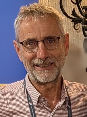
Could you introduce yourself, your research topic, and your role within the FAMES project?
I am Gabriel Parès, a research engineer at CEA-Leti with a background in material science and semiconductor technologies with over 33 years of experience in semiconductors and MEMS, including different former positions at STMicroelectronics, MEMScap, and CEA-Leti. I’m now leading the Work Package dedicated to embedded Non-Volatile Memories (eNVM) in the FAMES Pilot Line. My role involves coordinating the development of advanced memory technologies—such as OxRAM, FeRAM, FeFET, and MRAM—integrated into FD-SOI CMOS nodes such as 22FDX from Global Foundries and ultimately in FD10 and FD7 and to enable disruptive architectures using those eNVM for applications such as AI, cybersecurity, and energy-efficient computing.
The FAMES project aims to integrate several types of embedded Non-Volatile Memories (eNVM) within FD-SOI technologies. What are the main challenges your team is addressing, and why is embedded memory integration so important for future semiconductor applications?
The primary challenges of this work package include scaling eNVM technologies to 10nm and 7nm FD-SOI nodes, ensuring BEOL compatibility, and optimizing performance, reliability, and energy efficiency for diverse applications focused on Artificial Intelligence at the edge and security. For instance, FeRAM requires 3D capacitor integration to obtain a memory density better than SRAM at a given node, while OxRAM demands precise control of conductive filament formation for achieving the optimum endurance and retention. Embedded memory integration is critical because it reduces the “memory wall” bottleneck—where data movement between memory and logic consumes excessive power and latency. By co-integrating eNVM directly into the BEOL stack, we enable in-memory computing (IMC), reducing energy overhead and accelerating AI/ML workloads, which is essential for edge devices and IoT applications. As a consortium of different European research stakeholders, we address a broad range of activities from material engineering to design of circuit demonstrators around these different eNVM technologies.
Your Work Package explores different memory technologies, including OxRAM, FeRAM, FeFET, and MRAM. Why is it important to develop several complementary memory solutions rather than a single technology?
Each eNVM technology has its own strengths and is suited to different applications. OxRAM offers low-cost, high-density storage, although endurance can be a limitation. FeRAM combines high speed and low energy consumption. It also offers strong scalability potential, especially with 3D capacitor structures. MRAM stands out for its high endurance and speed. This makes it a good candidate for cache replacement. FeFET enables non-volatile logic with very low power consumption. It is particularly promising for applications such as neuromorphic computing. By developing complementary solutions, FAMES ensures that different use cases—from AI accelerators to cybersecurity (e.g., TRNGs and PUFs)—can leverage the best-fit technology. This diversity also mitigates risks if one technology encounters integration or performance hurdles.
What are the most significant achievements or breakthroughs obtained so far within your Work Package?
Over the past two years, our Work Package has made remarkable strides in several areas.
Our work on OxRAM has led to the development of an 8Mbit IP module in GF 22FDX, achieving a bit error rate (BER) of less than 1E-4 after 10k of endurance cycles. We have also realised a design-technology co-optimization (DTCO) study to scale the OxRAM bitcell beyond 22nm towards 10FD-SOI showing that this technology will be competitive in density with respect to finFET counterpart.
Regarding FeRAM, for the first time ever, we have successfully integrated a 3D FeCap into a 22nm CMOS node Back-End-of-Line (BEOL), achieving an impressive endurance of up to 10¹⁰ cycles and demonstrating high remnant polarization in some high aspect ratio via structures. This confirms the scalability of our technology for dense memory arrays. Additionally, a 32Mbit FeRAM macro has been designed in 22nm FD-SOI, with fabrication set to begin by the end of 2026 with our new Memory Advanced demonstrator shuttle MAD305.
In the field of MRAM, we have designed and tested stochastic Magnetic Tunnel Junction (sMTJ)-based True Random Number Generator (TRNG) circuits, achieving 10ns switching times and an energy consumption of 5pJ/bit. For this technology, the tape-out conducted by imec is planned for Q3 2026 also on GF 22FDX.
Furthermore, we have achieved the first Fe(M)FET technologies demonstrations at wafer scale, based on HZO ferro stack and oxide semiconductor (OSC) channel FET devices, both at VTT and at CEA-Leti. University of Granada (UGR) has also showcased wafer-scale PE-ALD growth MoS₂ and WS₂ and laser annealed devices at temperatures below 450°C for sensing and computing applications.
How do these embedded memory technologies open new opportunities for emerging applications such as artificial intelligence, cybersecurity, or energy-efficient computing?
Embedded non-volatile memories (eNVMs) pave the way for disruptive architectures by bringing memory closer to computation. In the realm of AI at the Edge, FeRAM-based Compute-in-Memory (CIM) arrays can significantly reduce data movement, cutting energy consumption for Deep Neural Networks (DNNs) and Large Language Models (LLMs) by orders of magnitude. For instance, Université Catholique de Louvain (UCL) has produced some primitive analog CIM macro with RISC-V control, aiming to demonstrate this concept, likewise, Fraunhofer has designed a primitive circuit based on FeMFET device targeting a CIM accelerator, both circuits are embedded in our MAD305 shuttle.
In cybersecurity, OxRAM’s intrinsic stochasticity is leveraged for True Random Number Generators (TRNGs) and Physical Unclonable Functions (PUFs), a focus area of Warsaw University of Technology (CEZAMAT-WUT) in our work package. Also, stochastic MTJ devices provide hardware-level randomness for secure key generation as well.
For energy efficiency, BEOL FeFETs and TMD transistors enable new schemes of computing like based on CIM and neuromorphic with ultra-low power consumption. Moreover, 3D integration through chip-to-wafer hybrid bonding included in our MAD305 shuttle allows for chiplet-based memory-logic stacking, optimizing bandwidth and power for heterogeneous systems.
How does the FAMES Pilot Line contribute to accelerating the development and validation of these eNVM technologies?
The FAMES Pilot Line is playing a pivotal role in accelerating the development and validation of embedded non-volatile memory (eNVM) technologies. By providing a 22FDX-based ecosystem with Memory Advanced Demonstrator (MAD) shuttles, such as MAD304 and MAD305, the Pilot Line facilitates rapid prototyping and validation. This environment allows our partners to access Process Design Kits (PDKs) and test vehicles, such as CEA-Leti’s FeRAM PDK for Fraunhofer and UCL designs for instance, fostering a collaborative approach to innovation.
Cross-partner collaboration is another key contribution of the FAMES Pilot Line. For example, imec, VTT, and UGR are benchmarking materials like MoS₂ versus IGZO for BEOL FeFETs, while CEZAMAT-WUT and CEA-Leti are co-developing OxRAM for AI and security applications. This collaborative effort ensures that the technologies are manufacturing-ready for European foundries through tape-outs such as actual MAD304 and next MAD305 planned for Q3 2026 with full compatibility to industry grade CMOS nodes as GF 22FDX.
One of the ambitions of FAMES is to enable disruptive IC architectures. How could the integration of advanced embedded memories change the way future chips are designed?
The integration of advanced embedded memories has the potential to revolutionise the design of future chips, enabling disruptive IC architectures that redefine the memory hierarchy. In-Memory Computing (IMC) is one such innovation that eliminates the von Neumann bottleneck by performing analog Multiply-Accumulate (MAC) operations directly in memory. For instance, FeRAM CIM arrays for Deep Neural Networks (DNNs) can significantly enhance processing efficiency. Non-Volatile embedded memories enable extremely low power consumption by retaining state without power, making them particularly suited for edge devices and IoT applications.
Monolithic 3D ICs, enabled by hybrid bonding and BEOL integration, allow for stacking memory and logic dies. This advancement reduces latency and power for high-bandwidth applications, opening up new possibilities for chip design. Furthermore, heterogeneous integration, which combines OxRAM (storage), FeRAM (CIM), and MRAM (cache) in a single chip, optimises Performance, Power, and Area (PPA) for domain-specific accelerators. This holistic approach to chip design is set to transform the semiconductor industry, making future chips more efficient, powerful, and versatile.
How do you see the impact of this work on Europe’s semiconductor ecosystem and on the development of future generations of FD-SOI-based technologies?
The work being conducted within the FAMES project is poised to have a profound impact on Europe’s semiconductor ecosystem. By accelerating the development of FD-SOI technologies, we are demonstrating the potential of embedded non-volatile memories (eNVM) as add-ons to 22FDX and then to FD10. This makes FD-SOI more competitive against FinFET for edge AI and IoT applications, strengthening Europe’s position in the global semiconductor market.
Fostering industrial collaboration is another key aspect of our work. Partnerships with GlobalFoundries and close collaboration among leading European Research and Technology Organizations (RTOs) such as imec, Fraunhofer, and VTT anticipate High-Volume Manufacturing (HVM)-ready solutions. Our approach also aims at opening access to these emerging technologies European Integrated Device Manufacturers (IDMs) and fabless companies, further enhancing the European semiconductor ecosystem.
Moreover, our efforts in training the next generation through winter schools and open-access MAD shuttles are building expertise in eNVM design and characterization for both academia and industry. This investment in human capital is crucial for the long-term sustainability and growth of the semiconductor industry in Europe. Additionally, enabling green electronics through low-power eNVMs aligns with EU sustainability goals, reducing energy consumption in data centres and edge devices. This work is not just about technological advancement; it is about shaping a sustainable and competitive future for Europe’s semiconductor industry.
What are the next key milestones and challenges for your team in the coming months?
In the coming months, our team is focused on several key milestones and challenges that will shape the future of our embedded non-volatile memory (eNVM) technologies. One of our primary goals is to achieve tape-outs, including CEA-Leti MAD305 and imec 22FDX MRAM shuttle in the second half of 2026. These tape-outs are crucial for the development of FeRAM macros, CIM demonstrators, and MRAM TRNG circuits, as well as the progresses in the integration of our technologies such as 3D FeCap process compatible with BEOL with the processing of the first silicon batches. This phase of our work is critical for validating our technologies and moving them closer to industrialisation. We are also pursuing technology reliability assessments based on the previous MAD304 batches. This iterative process of optimisation and assessment is essential for ensuring the robustness and reliability of our technologies. Furthermore, we are continuing the development of BEOL (Fe)FET technologies based on HZO for ferro materials, as well as oxide semiconductors (OSC) or transition metal dichalcogenides (TMD) for channel materials at VTT, UGR, and CEA-Leti. Continuous sharing of learnings among our partners is crucial for advancing these technologies and overcoming the challenges that lie ahead.
Gabriel PARES, CEA-Leti, Research Engineer and FAMES Embedded Non-Volatile Memories (eNVM) Expert
Find out more about the FAMES consortium.


