
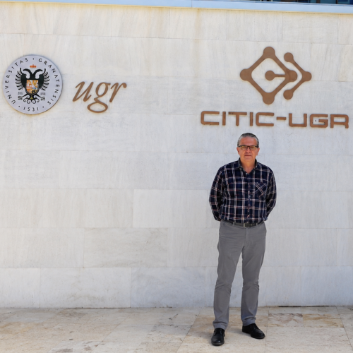
Francisco Gamiz, Professor at the University of Granada, specializes in integration of 2D materials for advanced semiconductor technologies. Within FAMES, he is developing a 2D-material platform aimed to be compatible with industrial CMOS processes. He discusses in this interview the challenges and opportunities of such integration.
At the University of Granada (UGR), our research focuses, among other topics, on the integration of two-dimensional (2D) materials into advanced semiconductor technologies. We investigate the growth, fabrication, characterization, and modeling of electronic devices based on transition metal dichalcogenides (TMDs), such as MoS₂ and WS₂, with particular emphasis on their integration into the Back-End-Of-Line (BEOL) of FD-SOI technologies.
Within FAMES, UGR contributes to the development of a 2D-material platform compatible with industrial CMOS processes. Our objective is to demonstrate wafer-scale growth of 2D materials, fabricate transistors and memory devices directly on CMOS-compatible substrates, and ultimately enable new More-than-Moore functionalities such as embedded non-volatiles memories, new memory concepts (embedded 1TDRAM cells, sensors for IoT (environment, bio, health), neuromorphic devices for in-memory computing, optoelectronics, and RF applications.
2D materials offer a unique combination of properties that make them highly attractive for future FD-SOI technologies.
First, their atomically thin nature provides excellent electrostatic control, enabling aggressive device scaling while reducing short-channel effects. Second, they can be integrated at relatively low temperatures, making them compatible with BEOL processing and therefore suitable for monolithic 3D integration. Third, they introduce functionalities that are difficult to achieve with conventional silicon alone, including sensing, non-volatile memory, neuromorphic computing, and optoelectronic applications.
From a manufacturing perspective, 2D materials offer the possibility of adding new device layers directly on top of completed CMOS circuits, thereby increasing functionality without increasing the chip footprint or disrupting mature CMOS fabrication processes.
Despite their enormous potential, several challenges still limit the industrial adoption of 2D materials.
One of the main challenges is achieving wafer-scale growth with sufficient material quality while remaining within the strict thermal budget required by CMOS technologies. Low-temperature deposition methods often result in polycrystalline films with defects, grain boundaries, and limited carrier mobility.
Another challenge is controlling the electrical properties of the devices, including contact resistance, Schottky barriers, defect densities, hysteresis, and long-term reliability. Last but not least, scalable integration requires robust lithographic processes, passivation strategies, and process flows that are fully compatible with industrial semiconductor manufacturing, while avoiding contamination of the previously processed FDSOI/CMOS system.
Our team is working on all these aspects, combining materials growth, advanced characterization, device fabrication, and simulation to establish a complete technological platform.
FAMES has provided an exceptional framework for accelerating our developments and aligning them with industrial requirements.
Over the last months, we have successfully demonstrated wafer-scale fabrication of MoS₂ transistors directly grown by Plasma-Enhanced Atomic Layer Deposition (PE-ALD) at temperatures compatible with BEOL integration. These devices exhibit stable ambipolar operation and low Schottky barrier heights, demonstrating the feasibility of CMOS-compatible 2D electronics. Although the performance of the fabricated devices still needs to be improved, this represents an important first step.
In parallel, we have demonstrated robust p-type WS₂ devices fabricated through a scalable growth process. Achieving reliable p-type behavior in sulfur-based TMDs is an important milestone because it enables complementary device architectures using the same material platform.
FAMES has enabled close collaboration with leading European semiconductor organizations, providing access to industrial requirements, integration roadmaps, and future pilot-line opportunities. This interaction is helping us transition from laboratory-scale demonstrations toward technologies that can be transferred into future manufacturing environments.
Our next objective is to further improve the quality and performance of low-temperature-grown 2D materials.
We are currently developing advanced post-deposition treatments, including thermal and laser annealing techniques, to reduce defect densities and enhance carrier mobility while maintaining CMOS compatibility. We are also expanding our work toward the demonstration of memory devices, sensors, and heterogeneous 3D integration schemes based on 2D materials.
Looking ahead, our goal is to establish a complete BEOL-compatible 2D technology platform that can be integrated into future FD-SOI pilot lines, enabling new generations of energy-efficient and multifunctional semiconductor systems.
Ultimately, we believe that 2D materials will play a key role in extending semiconductor innovation beyond traditional scaling, and FAMES is providing the ideal ecosystem to make that transition possible.
Find out more about the FAMES consortium.

Website designed and made by Perceptiom and FAMES

FAMES is a European Union’s Horizon Europe Research and Innovation programme
Website designed and made by Perceptiom and FAMES

Website designed and made by Perceptiom and FAMES
Ferrite Circulators: Theory, Design and Simulation
12 October 2026
Cost: 150€
All FAMES Partners undertake to respect their obligations in application of regulations in force and, especially, regulation (EU) 2016/679 of the European Parliament and of the Council of 27 April 2016, on the protection of natural persons with regard to the processing of personal data and on the free movement of such data (referred to as “GDPR”).
Keep up to date with the latest news from FAMES
All FAMES Partners undertake to respect their obligations in application of regulations in force and, especially, regulation (EU) 2016/679 of the European Parliament and of the Council of 27 April 2016, on the protection of natural persons with regard to the processing of personal data and on the free movement of such data (referred to as “GDPR”).
Request submitted!
Thank you for your registration. You will receive a copy by email. We will be getting in touch with you shortly to confirm or not your registration to the Winter school.
If you encountered an error or did not receive a copy (please check your spam), contact us.
FAMES European FD-SOI Design School (EFDS)
FAMES European FD-SOI Design School (EFDS)
January 25-29, 2027
Training costs: 1400€
All FAMES Partners undertake to respect their obligations in application of regulations in force and, especially, regulation (EU) 2016/679 of the European Parliament and of the Council of 27 April 2016, on the protection of natural persons with regard to the processing of personal data and on the free movement of such data (referred to as “GDPR”).
Request submitted!
Thank you for your request. You will receive a copy by email. We will be getting in touch with you shortly.
If you encountered an error or did not receive a copy (please check your spam), contact us at open-access-chair@fames-pilot-line.eu.
FAMES Open-Access Call User Request
Please note that your answers will help us establish the eligibility of your request.
All FAMES Partners undertake to respect their obligations in application of regulations in force and, especially, regulation (EU) 2016/679 of the European Parliament and of the Council of 27 April 2016, on the protection of natural persons with regard to the processing of personal data and on the free movement of such data (referred to as “GDPR”).
Spontaneous User Request
Please note that your answers will help us establish the eligibility of your request.
All FAMES Partners undertake to respect their obligations in application of regulations in force and, especially, regulation (EU) 2016/679 of the European Parliament and of the Council of 27 April 2016, on the protection of natural persons with regard to the processing of personal data and on the free movement of such data (referred to as “GDPR”).
Contact

Susana Bonnetier (CEA-Leti)
For inquiries or problems regarding the Open Access/Spontaneous Request, you can contact us directly.
Trainings
Annual call