
Dominique Noguet
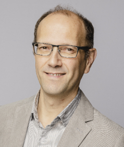 Dominique Noguet is the coordinator of the FAMES Pilot Line, and VP at CEA-Leti. Prior to this role he held several positions as digital IC designer, lab manager and department manager. He led many projects at a national level and in European frameworks (FP5, FP6, FP7), and large industrial partnerships. Dominique has authored or co-authored 100+ scientific papers (several best paper awards), several book chapters and 15 patents. He was a reviewer and a member of scientific committees of international conferences and a member of journal editorial boards. He was conference chair and TPC chair of several international conferences, and is an IEEE Senior Member. Dominique holds an engineering degree of the National Institute of Applied Sciences (INSA) in electrical engineering in 1992, and a PhD from National Polytechnical Institute of Grenoble (INPG) in 1998.
Giorgos fagas
 Pr Giorgos Fagas (PhD, MBA) is Director of Strategic Development at Tyndall National Institute and a member of its Executive Leadership Team, where he shapes the institute’s international strategy and leads major cross-cutting initiatives. An expert in advanced semiconductors, nanoelectronics and quantum technologies, he has played a central role in European research and innovation, contributing to Ireland’s Silicon Island strategy and the EU Chips Act through the implementation of pilot lines such as FAMES, horizon scanning and coordinating numerous EU-funded projects. Advancing international collaboration, expanding pilot line activities, and driving technology foresight efforts that strengthen Europe’s semiconductor ecosystem and global partnerships, Giorgos is the Director of SiNANO and coordinator of the ICOS2 EU Coordination and Support Action on ‘International Cooperation on Semiconductor Innovation and Supply Resilience’.
Thierry Poiroux
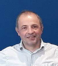 Thierry Poiroux received the M.S. degree from Ecole Centrale Paris, France, in 1995 and the Ph.D. degree from the University of Nantes, France, in 2000. After a Ph.D. work carried out at the Commissariat à l’Énergie Atomique/Laboratoire d’Electronique et de Technologie de l’Information (CEA–Leti), Grenoble, France, and Matra MHS on plasma process-induced damage, he joined CEA–Leti as a Research Staff Member in 2000. Until 2002, he was involved in partially and fully depleted silicon-on-insulator (SOI) process integration and compact modeling. From 2002 to 2010, he worked on advanced device architectures and was in charge of multiple-gate device modeling, planar double gate process integration and fabrication of graphene-based transistors. In 2011 and 2012, he has been the Head of the Innovative Device Laboratory of CEA–Leti, dedicated to the development of advanced CMOS technologies. From 2012 to 2018, he developed the second version of the L–UTSOI compact model, selected by the Si2 Compact Model Coalition as a standard industrial model for fully-depleted SOI technologies. From 2018 to 2021, he was the head of the Simulation and Compact Model Laboratory of CEA–Leti. From 2021 to March 2025, he was in charge of the Characterization, Design and Simulation Department, and he is currently project leader. He has authored or coauthored five book chapters and about 190 papers and communications, and he is author or co-author of about 20 patents.
Valeriya Kilchytska
 Valeriya Kilchytska is Senior Researcher, Logistic Director assuring scientific lead of the WELCOME Electrical Characterization Platform at UCLouvain. She received her PhD degree in semiconductor and dielectric physics from Taras Shevchenko National University of Kyiv, Ukraine in 1997. Her PhD work is on the electrical and radiation properties of Silicon-on-Insulator (SOI) structures. Then she worked at Kyiv Institute of Semiconductor Physics on the bias-temperature processes in SOI. In 2001, she was a visiting researcher at the Chalmers University of Technology, Sweden, for characterization of SiC MOS structures. She joined UCLouvain in 2002. She has a long-term experience in characterization, simulation and modelling of advanced devices with a focus on wide frequency band and noise characterization, performance assessment as well as cryogenic, high-temperature and radiation behavior. She has authored or co-authored > 300 scientific papers and conference contributions. She is a reviewer for numerous scientific journals and a TPC member of several conferences. Since 2023, she is a Deputy Director of SINANO Institute.
Gabriel Parès
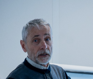 Gabriel Parès has an Engineer degree in “material science” from l’Institut National des Sciences Appliquées (INSA) de Lyon, France and a postgraduate degree in “semiconductor material sciences” from the University of Lyon.
He has been working for 33 years in semiconductors and MEMS industry in industrial and R&D fields, formerly for STMicroelectronics and MEMScap, then he joined CEA-leti in 2004.
He has been working from 2010 to 2020 in the field of 3D integration and advanced packaging technologies. Since 2021 he is project manager in the Laboratory of Memories and Computing in charge of the work package dedicated to embedded Non Volatile memories of the FAMES pilot line. He holds 18 patents and he is the author of 19 publications in different fields of semiconductors technologies.
Piotr Wisniewski - CEZAMAT
Abstract : This presentation explores the design of reliable RRAM-based Physically Unclonable Functions (PUFs) for hardware security. By exploiting the intrinsic stochastic variability of resistive switching, RRAM devices generate unique cryptographic signatures for authentication and secure key generation. We focus on reliability challenges, addressing response reproducibility and other aspects to ensure stable, repeatable outputs. RRAM optimized control scheme is also explored. The non-volatile, CMOS-compatible nature of RRAM enables robust, low-power root-of-trust primitives for next-generation secure IoT, embedded, and edge computing applications.
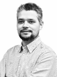
Piotr Wiśniewski, Ph.D. Eng., is a Head of Intelligent Semiconductor Systems Division (SEMINSYS), Centre for Advanced Materials and Technologies CEZAMAT, Warsaw University of Technology. He received his MSc. Eng. degree in microelectronics, photonics, and nanotechnology, and a Ph.D. degree in electrical engineering from Warsaw University of Technology (WUT). Currently is the Head of the Intelligent Semiconductor Systems Department (SEMINSYS) and an assistant professor at the Centre for Advanced Materials and Technologies CEZAMAT WUT, responsible for managing the semiconductor technology line and R&D activities of the department. His research interests and expertise cover physics, modeling, and technology of semiconductor devices for micro / nano-electronics and photonics. He has been actively involved in national and international projects as a principal investigator or researcher, supported by various research agencies
Alexandre Reinhardt
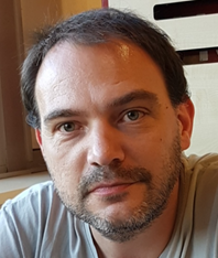 Alexandre Reinhardt is a senior technical expert with 25 years of experience in developing acoustic wave resonators and filters for the wireless communication industry. After a PhD at the FEMTO-ST Institute (Besançon, France) sponsored by Temex (now Qualcomm France), he joined CEA-Leti in 2006. His research focuses particularly on bulk acoustic wave resonators, their modeling and the design of these devices, to answer the need to continuously increase operation frequencies and quality factors. In the past decade, he has particularly investigated the use of single crystal highly piezoelectric materials such as lithium niobate, which now find applications in the filtering industry.
Daphnée Bosch
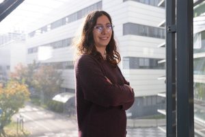 Daphnée Bosch received the M.Sc. degree in micro and nanotechnologies for integrated systems from Grenoble-INP Phelma, Politechnico di Torino and EPFL in 2017 and the Ph.D. degree in microelectronics from the University of Grenoble-Alpes in 2020. Her current research interest is advanced CMOS technologies, focusing on 3D sequential integration and fully depleted SOI devices. She has authored over 25 papers in international conferences or journals in this field and has been part of the IEDM process technology committee. Currently, she is in charge of 400°C low temperature devices development in the FAMES project.
Emmanuel Ollier
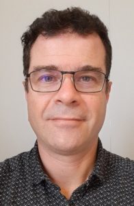 Dr. Emmanuel Ollier is the EU Program Manager at CEA-Leti’s Semiconductor Components Division. Previously, he led the Laboratory of 3D Integration and Advanced Packaging Technologies at CEA-Leti. With 17 years of experience in the semiconductor industry (including roles at Thales, Atmel, NXP, EM Microelectronics) he holds 22 patents and has authored 45 papers and international conference presentations. Dr. Ollier earned a PhD in Material Sciences and an Engineering Degree from the French National School of Physics and Chemistry of Bordeaux. His expertise focuses on the heterogeneous integration of semiconductor and photonic technologies, with applications spanning High-Performance Computing, Edge-AI, RF communications, smart sensors and displays, and power electronics.
Sambuddha Khan
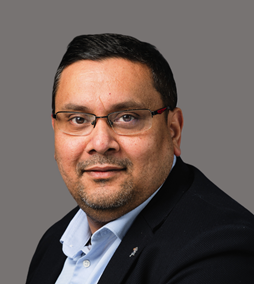 Dr Sambuddha Khan is a Senior Scientist and Technical Lead at Tyndall National Institute, Ireland, where his research focuses on the design, fabrication, and heterogeneous integration of MEMS and micro-components, including integrated magnetics, piezoelectric transformers, and AlScN-based RF acoustic resonators for power-supply-on-chip applications. He serves as Programme Manager for Tyndall’s participation in the Chips JU FAMES Pilot Line project and has led research programmes funded by Horizon Europe, Research Ireland, and Enterprise Ireland. Before joining Tyndall, he was a postdoctoral researcher at the University of California, Irvine, working on a DARPA-funded programme on inertial-grade silicon MEMS gyroscopes. Dr Khan received his PhD from the Indian Institute of Science, Bengaluru, in 2014, and lectures at University College Cork on MEMS and microfabrication.


