
Contact Punch-Through Failure Mitigation for Advanced FD-SOI Nodes
The study explores the mitigation of contact punch-through failures in advanced FD-SOI nodes by introducing a thin SiCO layer beneath the contact etch stop layer. We demonstrate that this integration optimization significantly improves contact robustness and therefore relaxes contact placement constraints within the device active region, offering a cost-effective solution to alleviate interconnect congestion in advanced FD-SOI nodes.
Due to advanced technology node scaling, integrated circuit design faces back-end of line (BEOL) congestion issues, with potential penalties on total wirelength, logic cell count, and chip area. The use of local interconnect at middle of line (MOL) levels, where contact plug extends beyond the edge of the active region, can alleviate this congestion. However, for FD-SOI technologies, such strategy increases the risk of contact punch-through, which may result in device malfunction and circuit yield loss.
CEA-Leti investigated the benefits of adding a thin layer of a dedicated dielectric material under the SiN contact etch stop layer (CESL), to prevent contact punch-through. Several materials were studied based on their wet etch rate, etch selectivity, permittivity and mechanical stress. Among these, SiCO was identified as the most promising anti punch-through (APT) candidate.
We evaluated the SiCO layer efficiency on contact punch-though mitigation using a 28FD-SOI-like manufacturing flow with a 5nm SiCO layer added before SiN CESL deposition. Intentional contact misalignment with respect to the active region (RX) was also performed to force punch-through occurrence, resulting in three distinct contact position (inside, edge and outside).
Electrical results show that the leakage current between contact and substrate is similar for both reference and SiCO samples when the contact is located within the active region, but strongly diverges otherwise. A current increase of almost two decades and a higher spreading is observed for the reference case, whereas it remains at the same value regardless of the contact position with the SiCO layer, demonstrating clear evidence of increased robustness brought by the SiCO layer.
Breakdown voltage (VBD) measurements further illustrate the remarkable robustness gain with SiCO, leading to VBD around 15V for extreme contact position compared to values way below 5V for the reference process. As a consequence, a 100% breakdown yield is maintained with the SiCO layer regardless of contact position whereas it dramatically drops for reference process, when the contact is shifted outside of the active region. TEM cross-sections confirm the SiCO layer prevents the contact from extending downwards even when spanning over the active edge, thus efficiently preventing contact punch-through occurrence.
This approach effectively relaxes contact placement constraints within the active area, offering a cost-effective solution for advanced FD-SOI nodes, relieving M1 congestion and enhancing overall chip design efficiency. These results represent a key milestone for the FAMES project, demonstrating a significant step forward in extending the FD-SOI technological roadmap toward future advanced nodes.
Illustrations:
Figure 1: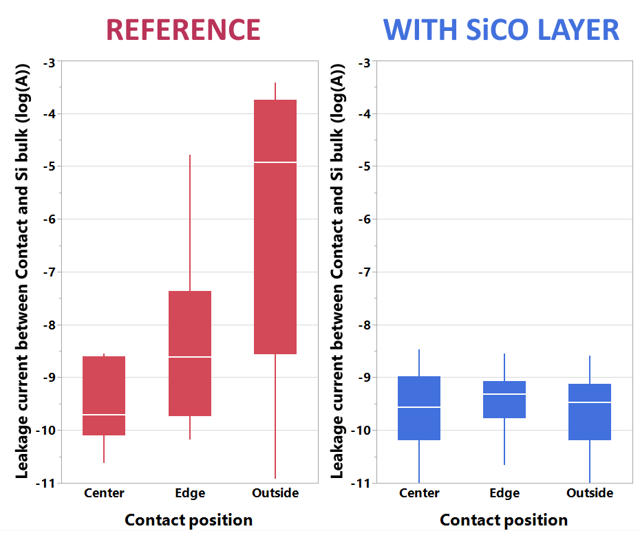
Figure 2:
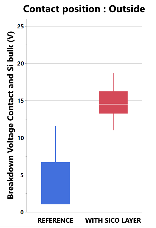
Figure 3: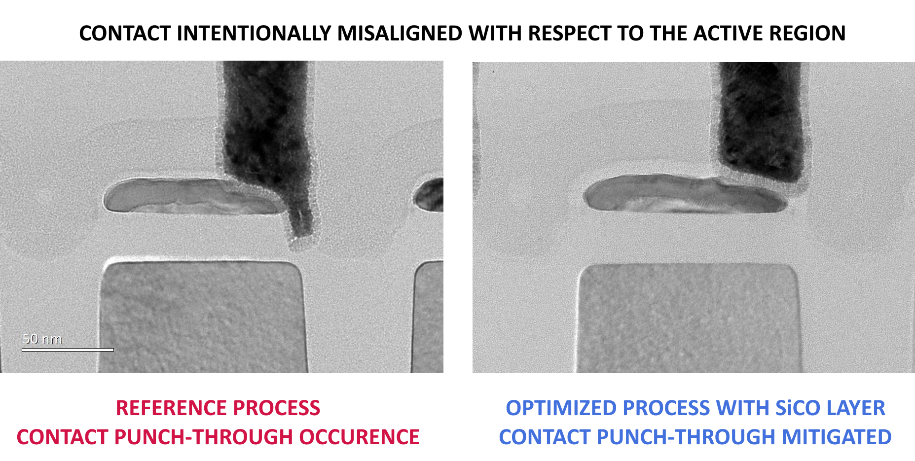 :
:
Scientific contacts and contributors
E. Petitprez, P. Brianceau, A. Krakovinsky, K. Romanjek, Y. Maneglia, O. Billoint, J. Nacenta-Mendivil, B. Mohamad, Z. Chalupa, M. Charbonneau, O. Cueto, A. Boujnah, F. Bringuier, M. Bedjaoui, V. Lapras, F. Aussenac, L. Couture, A. Magalhaes-Lucas, G. Garnier, B. Duriez, M-C. Cyrille and C. Fenouillet-Beranger
Contact person for follow-up
E. Petitprez, CEA-Leti
Explore FAMES technologies
Find out more about FAMES Power Management of Integrated Circuits


