Ferroelectric HfO2/ZrO2 Superlattice Capacitors with High Center to Edge Wafer-Scale Uniformity
VTT demonstrated high wafer-scale uniformity for ferroelectric HfO₂/ZrO₂ capacitors on a 150 mm wafer, taking important steps towards pilot-line fabrication of low-power non-volatile memories. Developed within the EU FAMES pilot line, the results showcase how it is possible to reduce the impact of overall process variations by tuning the thickness of the ferroelectric sublayers.
Contemporary large capacity memory technologies have become a severe bottleneck in AI computations due to the high energy consumption associated with volatile memory states. The semiconductor industry is thus under growing pressure to deliver memory technologies that can combine non-volatile properties with high performance, low power operation, and a small integrational footprint. Non-volatile memories (NVMs) based on ferroelectric HfO₂ materials have the potential to fulfill all of those aspects and are especially attractive because they are compatible with established Si-CMOS processes. However, when scaling the thickness of the ferroelectric layer to allow for low voltage switching and dense integration, maintaining tight electrical uniformity across a full wafer becomes challenging due to the thin layers being sensitive to various process variations. Finding stable process conditions is therefore essential to commercialize ferroelectric HfO₂ NVMs.
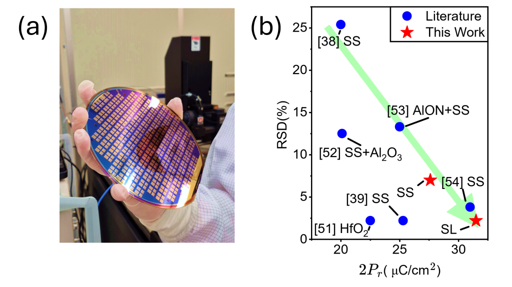
In this work, ferroelectric HfO₂/ZrO₂ (HZO) metal-insulator-metal (MIM) capacitors with different sublayer thicknesses are characterized to investigate the impact on wafer scale performance distributions (see Figure 1a). The study includes standard solid solution HZO (SS-HZO, alternated every 1 atomic layer) and superlattice HZO (SL-HZO, alternated every 6 atomic layers). It has been shown in the literature prior that the ferroelectric performance of individual devices can be improved by implementing SL-HZO. Our findings take this one step further, that by implementing SL-HZO, the co-variance to process variations across a wafer is significantly reduced, with robust switching behavior from the center to the edge, showcasing state-of-the-art performance (see Figure 1b).
The processing of the samples in the study was performed in the OtaNano Micronova cleanroom in Espoo, Finland, as part of VTT’s development of a NVM pilot-line within the EU FAMES project. To improve our characterization capabilities, VTT has acquired new parameter analyzers that were procured within the FAMES project last year, and these are now in heavy use. Another important aspect in developing our pilot-line is tight process control, where a focus on yield and uniformity is of high priority. Increased in-line monitoring is part of that work. The now demonstrated wafer-scale uniformity is particularly relevant for building a future back-end-of-line (BEOL) NVM platform aiming toward stable pilot-line processing and industrial benchmarking.
The next steps include co-integration with a BEOL selector device, substantial footprint scaling, as well as continued improvement of yield and process repeatability. A VTT NVM platform could be implemented in BEOL compute-in-memory solutions but also offer customers a high degree of flexibility for innovative explorations.
References
O.Kaatranen, P.Eskelinen, S.Inkinen, O.-P.Kilpi, and K.-M.Persson, “Ferroelectric HfO2/ZrO2 Superlattice Capacitors With High Center to Edge Wafer-Scale Uniformity.” Advanced Electronic Materials12, no. 10 (2026): e00773. https://doi.org/10.1002/aelm.202500773
Scientific contacts and contributors
Oscar Kaatranen (VTT), Karl-Magnus Persson (VTT)
Explore FAMES technologies
Find out more about FAMES Embedded non-volatile memory.
