SADP implementation at the gate-level patterning for the 7nm FD-SOI node
This work validates the integration of a Self-Aligned Double Patterning (SADP) approach to fabricate FD-SOI gates with aggressive dimensions (CPP = 57 nm, Lg = 20 nm) within the FAMES project. A key aspect was the optimization of the material stack, including mandrel, SiO₂ spacers, and hard masks, combined with highly selective dry and wet etching processes. These results demonstrate the feasibility of extending planar FD-SOI technology toward 7nm node using a low-cost patterning solution such as SADP.
FD-SOI planar technology is an alternative to the FinFet in order to address a large range of applications (i.e. IoT, mobile applications, advanced power management and high RF/mmWave performance). Unlike FinFETs, where gate patterning is constrained by 3D fin topography requiring complex process steps, planar FD-SOI technology simplifies the integration flow. Indeed, gate patterning is performed on planar active surface. However, one of the key challenges in developing the 10 and 7nm FD-SOI technology platform is to achieve aggressive Contact Poly Pitch (CPP ≤ 68 nm) while maintaining a nominal gate length (Lg) of 20 nm with tight critical dimension control. Such scaling is essential to sustain device density improvements while preserving manufacturability on existing 193 nm lithography tool. In this context, Self-Aligned Double Patterning (SADP) has been selected as a key patterning strategy to limit lithography cost while enabling sub-80 nm pitch integration. In this study, a first SADP demonstration was carried out on an FD10-compatible gate stack, targeting a final pitch of 57 nm, representative of 7 nm technology nodes (according to the FAMES FD-SOI roadmap).
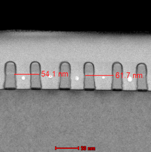
The SADP process successfully enabled a pitch reduction by a factor of two, resulting in FD-SOI gate structures with Lg = 20 nm and a final CPP of approximately 57 nm. A key aspect was the optimization of the material stack, including mandrel, SiO₂ spacers, and Etch Stop Layer (ESL)/SiO₂/SiN hard masks, combined with highly selective dry and wet etching processes. Initial challenges such as non-uniform etch depths after spacer formation were identified and mitigated by developing selective etching steps, enabling uniform and symmetric profiles. Spacer thickness was carefully tuned to ensure proper transfer into the hard masks and near-complete consumption during etching. The ESL hard mask was also selectively removed without degrading underlying layers, preserving critical dimensions. Final Transmission Electron Microscope (TEM) analysis confirms well-defined gate structures with vertical profiles and a gate length close to the target (21 ± 1 nm), demonstrating the scalability of planar FD-SOI technology.
This result represents a key milestone for the FAMES project, as it demonstrates the feasibility of extending FD-SOI technology toward 7 nm node using a low-cost solution such as SADP approach instead of relying on EUV lithography. It confirms that with the appropriate integration engineering, existing 193 nm-is a realistic path towards advanced FD-SOI manufacturing with aggressive critical dimensions. This strengthens the technological roadmap for FD10 and beyond, ensuring a viable path for future FD-SOI nodes.
Future work will focus on further optimizing etch profiles, reducing defectivity and pitch walking through improved mandrel CD control. In parallel, additional modules such as “multi-CD gate-level” and “cut-level” patterning using a cut-last strategy will be developed to produce co-integrated gates lengths and complete the full patterning scheme required for advanced node integration. The integration will also be extended to next-generation mask sets in order to implement into complete electrical lots this SADP process flow dedicated to planar 10-7nm FDSOI technology. One perspective will be also to evaluate and improve the environmental impact of SADP process flow by carrying out a Life Cycle Analysis.
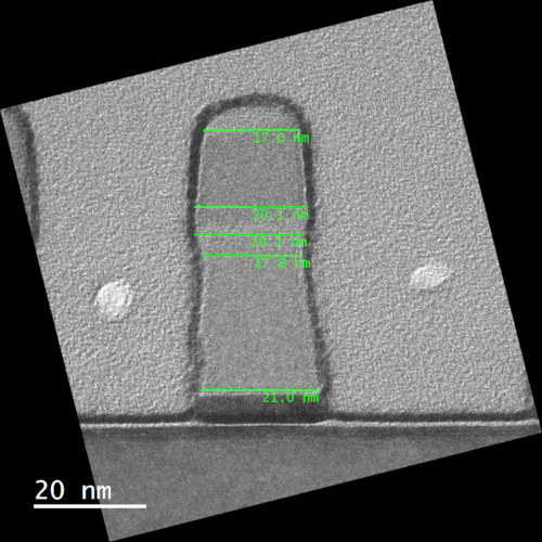
FD-SOI gate profile using the SADP technique with a final pitch of 57nm targeted for the 7nm node – © CEA-Leti
References
S. Beaurepaire et al, “Mandrel material selection as prerequisite for SADP implementation at the 10 nm FD-SOI node”, EUROSOI-ULIS 2026
M. Y. Aliouat, et al, “Plasma etching process tailoring for different polysilicon microstructures used in 10nm FD-SOI metal gate stacks,” Proc. SPIE 13984, 2026
C. Fenouillet-Beranger et al., “Pursuing the FD-SOI roadmap down to 10 nm and 7 nm nodes for high energy efficient, low power and RF/mmWave applications »,Solid State Electron, 231 (2026), Article 109264, https://doi.org/10.1016/j.sse.2025.109264
Scientific contacts and contributors
Patricia PIMENTA-BARROS, Sylvain BEAUREPAIRE, Mouaad-Yassine ALIOUAT, Lucie LARAIGNOU, Sakina YAHIAOUI, Gregory BONIFACE, Khadra HAMAMA, Jonathan PRADELLES, Aurélien SARRAZIN, Valérie LAPRAS, Marie-Claire CYRILLE, Claire FENOUILLET-BERANGER.
Explore FAMES technologies
Find out more about FAMES FD-SOI technologies
