FD-SOI

FD-SOI: a strategic EU-MADE technology, launched forward by FAMES
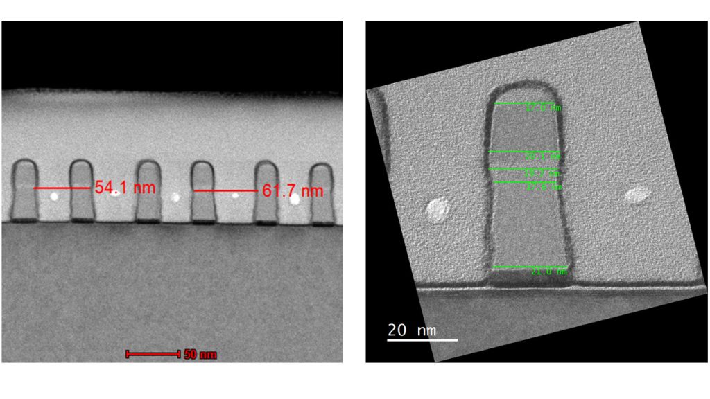
The Fully Depleted Silicon On Insulator, or FD-SOI, technology was developed in Grenoble by CEA-Leti, STMicroelectronics and Soitec. This planar process technology relies on two primary innovations: an ultra-thin layer of insulator (≤ 20nm, typically silicon dioxide), called the buried oxide (BOX), positioned on top of the base silicon substrate; a very thin silicon (Si) film (≤ 10nm), placed on top of the BOX layer, which will become the transistor channel.


FD-SOI is one of the currently widespread CMOS process technologies. FD-SOI is a planar technology where the transistor channel is located above a thin buried oxide, which helps control the channel from the gate. Minimizing the thickness of the top silicon layer above the BOX results in the absence of intrinsic charge carriers in the channel between the source and the drain contacts. Hence the name of “fully depleted” SOI.
The main advantages of this very thin silicon channel is the improvement of gate control on the channel resulting in lower leakage currents and better switching characteristics. With FD-SOI, the voltage applied to the gate can better control both the accumulation of carriers under the gate and the current flowing from the source to the drain.
An FD-SOI transistor’s electrostatic characteristics are similar to those of the FinFET technology and much better than those of conventional bulk Si technology. The buried oxide layer lowers the parasitic capacitance between the source and the drain making it possible for FD-SOI devices to operate at higher frequencies, lower operating voltages and better energy efficiency than equivalent FinFET devices. Once again, because the buried oxide film efficiently confines the electrons flowing from the source to the drain, performance-degrading leakage currents are dramatically reduced. The major advantages of FinFET, and the reason why it developed faster than FD-SOI, is a higher drive current per unit surface (thanks to the “3D channel”) which translates into a higher absolute performance in digital circuits. However, the reduced silicon geometries of the planar FD-SOI technology means that the same function can be implemented on a smaller silicon area and the chip design can be simplified compared to the FinFET technology, in particular for analogue and radiofrequency chips.
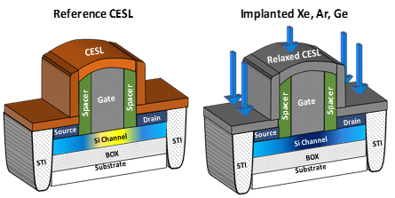
One of the major specific features of the FD-SOI technology is the ability to adjust the behavior of transistors not only through the gate, but also by polarizing the substrate underneath the device: this is called back biasing. Thanks to the ultra-thin insulator layer, back biasing can be used to dynamically adapt the operating regime between high performance/high speed and low power consumption/stand-by very efficiently. For example, in the case of a negative (NMOS) transistor, when the polarization of the substrate is positive, the operating frequency can be increased by increasing the transistor ON current. This is called “Forward Body Biasing” or FBB. If the substrate polarization is negative, the leakage current decreases with a resulting reduction of static energy consumption. This is called “Reverse Body Biasing” or RBB.
This feature makes FD-SOI an optimal technology for providing energy efficient integrated circuits. Easy to implement, FBB can be modulated dynamically during transistor operation, bringing much needed flexibility to Integrated Circuit design: circuits can be designed to operate faster when required and be more energy efficient when performance is not critical.
The combination of optimized digital characteristics and excellent analogue/RF behavior gives FD-SOI users the unique ability to co-integrate digital processing blocks and high-performance RF blocks in specialized circuits for applications like telecom (millimeter wave transceivers, 5G/6G systems) and automotive radars. Another advantage of the FD-SOI technology is its excellent radiation hardness to both single events and cumulated dose effects (the BOX neutralizes the charges generated by the radiation in the substrate and the thin layers of the device have very low carrier generation probability).
This characteristic is a key advantage for the automotive market, which needs to be resistant to radiation for safety reasons (e.g., ADAS application) and aerospace applications. Coupling FD-SOI with RRAM, in replacement of Flash or DRAM, is a smart choice for rad-hard circuits.
In spite of the very good performance obtained down to the 22nm node at the industrial scale (and 14 and 12nm at the experimental stage), it is obvious that more advanced FD-SOI nodes are required in order to remain competitive relative to sub-10nm FinFET technologies. Scaling down the FD-SOI technology to 10 and 7nm will lead to significant chip performance improvements compared to currently existing nodes, in terms of density, power consumption, speed and radiofrequency behavior. For example, device density is expected to be improved by a factor of three, power consumption by a factor of four and switching speed by a factor of two. With these performance improvements, the 10 and 7nm FD-SOI nodes will be very competitive in terms of digital performance compared to 7 and 5nm FinFET, still benefit from simpler process flows and lower manufacturing costs and better suitability for analogue and mixed signals circuits.
See more
- Technology
- Technology
- Technology
- Technology

- Technology

