
Impact of Device Position within the Silicon Active Area on Self-Heating and Thermal Coupling in FDSOI Transistors
As integrated circuits continue to scale down, higher device density and power dissipation turn self-heating and thermal coupling into critical challenges for advanced semiconductor technologies. In FDSOI devices, the buried oxide further exacerbates these thermal effects by limiting heat dissipation due to its low thermal conductivity. In this work, we experimentally investigate two identical FDSOI transistors located at different positions within the silicon active area: one located near the edge of the active region and another positioned more centrally. The results show that edge-positioned devices exhibit higher temperature rise and stronger thermal coupling due to reduced lateral heat spreading. This study was carried out within the framework of the FAMES Pilot Line collaboration between UCLouvain and CEA-Leti.
Advanced semiconductor technologies are increasingly affected by thermal limitations as transistor dimensions continue to shrink. In highly scaled CMOS circuits, localized temperature rise can lead to performance degradation, variability increase, and accelerated reliability issues. Among advanced technologies, FDSOI transistors offer strong electrostatic control and reduced parasitic effects thanks to the buried oxide (BOX). However, the BOX also acts as a thermal barrier that restricts heat dissipation from the channel.
While self-heating effects in FDSOI devices have been widely reported, the impact of transistor position inside the silicon active area on thermal behavior remains unexplored experimentally, to our best knowledge. Understanding these layout-dependent thermal effects is becoming crucial for future compact modeling, thermal-aware design, and reliable integration of highly dense circuits.
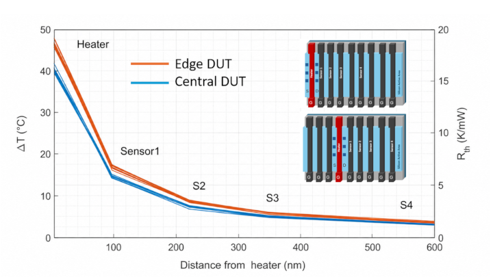
In this work, test structures realized by CEA-Leti within the framework of the FAMES Pilot Line, were experimentally characterized at UCLouvain using the gate resistance thermometry technique. The study compared two electrically similar LVT NMOS FDSOI transistors positioned at different locations within the silicon active area.
The measurements showed that transistors located near the edge of the silicon active area experience stronger self-heating and thermal coupling effects compared to more centrally positioned devices. The extracted temperature rise of the edge device was approximately 6.6 °C higher than that of the central device, highlighting the strong influence of transistor location and lateral heat spreading paths on thermal behavior in advanced FDSOI technologies.
The FAMES Pilot Line provided the collaborative framework and access to advanced FDSOI technology necessary for this research activity. The experimental measurements were carried out at the WELCOME platform of UCLouvain, combining the fabrication expertise of CEA-Leti with the thermal characterization capabilities and expertise of UCLouvain. This collaboration enabled the experimental investigation of position-dependent self-heating and thermal coupling effects in advanced FDSOI technology.
These results represent an important step for the FAMES project because they provide experimental insight into thermal effects in advanced FDSOI technologies at the layout level. The study demonstrates that transistor placement within the silicon active area can significantly influence self-heating and thermal coupling behavior, even for electrically similar devices. Such understanding is essential for improving thermal-aware device design, compact modeling, and the reliability of future highly integrated semiconductor circuits.
This work contributes to eco-innovation and sustainability by improving the understanding of thermal effects in advanced semiconductor technologies, which is essential for developing more energy-efficient and reliable integrated circuits. Better management of self-heating and thermal coupling can help reduce unnecessary power consumption, improve device lifetime, and limit reliability-related failures, thus contributing to more sustainable electronic systems and optimized resource utilization.
The outcomes of this work can support the development of thermal-aware design strategies for future FDSOI technologies and highly integrated CMOS circuits. The experimental results are particularly relevant for applications requiring high reliability and energy efficiency, such as automotive electronics, edge computing, RF systems, and low-power integrated circuits. The study can also contribute to improving compact thermal models used in circuit-level simulations and reliability analysis.
Future work within the project will focus on extending the experimental analysis to additional device geometries, layouts, etc to further investigate layout-dependent thermal effects in advanced FDSOI technologies. The next steps also include TCAD simulation and the integration of self-heating and thermal coupling effects into compact models for electrothermal simulations and reliability-oriented circuit design.
References
Oral presentation at the 12th EuroSOI-ULIS Conference, Granada, Spain, May 2026.
Scientific contacts and contributors
Sahebghalam (UCLouvain), M. Vanbrabant (UCLouvain), L. Lucci (CEA-Leti), Y. Zhang Fu (CEA-Leti), J.-P. Raskin (UCLouvain), V. Kilchytska (UCLouvain)
Explore FAMES technologies
Find out more about FAMES FD-SOI technologies


