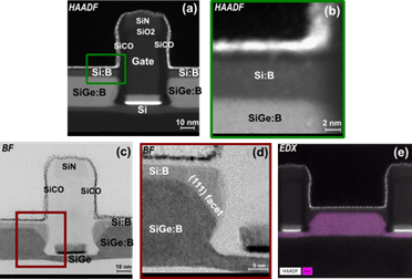
In the frame of FAMES, the development of a first generation of SiGe:B, with approximately 30% of germanium has provided a solid starting point for evaluating pMOS device performance.
In advanced nodes, aggressive scaling significantly increases parasitic access resistance through the source/drain electrodes and the junctions to the transistor channel. For the 10 nm FD-SOI node, efforts to enable higher and better-control of the doping region for reduction of resistivity are increasingly challenged by the constrained geometrical spacing (increased density). The physical downscaling of layers (reduction in silicon film and gate stack thickness) limits the effect of conventional approach of ion implantation and annealing. For this purpose, a new generation of source/drain epitaxy with in-situ doping is developed in order to enable direct and controlled integration and distribution of active dopants within the epitaxial layer. Beyond series resistance lowering, in-situ doped Sources and Drains (SDs) could also play a significative role in the transistors performance by inducing mechanical strain in the channel due to a change in lattice constant properties. Indeed, the Hole mobility will be higher in the compressively-strained channels of pMOS devices, while tensile strain will yield higher electron mobility in the channels of nMOS devices. In the frame of the FAMES project, our research focusses on increasing the active doping concentration and strain capability respectively for phosphorus doped silicon (Si:P) epitaxy for nMOS device and Silicon Germanium Boron doped (SiGe:B) for pMOS device while progressively assessing their integrability in CMOS devices.
The junction lies at the heart of the technological challenges associated with the FD-SOI transistor. Improving this junction, where epitaxy plays a major role, has a direct impact on both the static and dynamic electrical performance of the transistor. Achieving a high doping level in the source and drain are is mandatory to reduce the access resistance and to reach the 10nm FD-SOI specifications. Advanced in-situ doped epitaxy enables a precise control and localization of the dopants profiles while maintaining a high crystalline quality and activation ratio for very high doping levels. Epitaxy control gives the flexibility to define the morphology of the Source and Drain through facet formation to reduce the Gate-Source and Gate-Drain parasitic capacitance. Another way to improve the performance is the introduction of strain to boost the electron and hole mobility. Thus, the in-situ doped epitaxy is essential to improve both access resistance and carrier mobilities.
In the FAMES project, one of the tasks focuses on material and electrical characterization of the generations of in-situ doped epitaxy process developed to enhance FD-SOI transistors performance. A particular attention is given to the optimization of the doping profile within the source and drain and also to the control of dopant diffusion under the spacer.
SiGe:B epitaxy is developed for pMOS devices (compressive strain for holes mobility boost) and Si:P epitaxy (up to tensile layers for electrons mobility boost) for the nMOS.
SiGe:B optimizations were performed in order to: maximize the active boron concentration in epitaxy grown layers while preserving selectivity (i) versus SiN hard masks at the top of the gate as well as (ii) low-k sidewalls nitride based spacers. We worked on keeping a reasonable growth rate for a given germanium content. An Si:B capping layer was also developed to to ease the SiGe:B salicidation step on top of SiGe:B.
Regarding the NMOS Si:P epitaxy, first generations (from Gen 0.9 to Gen 1.4) aimed at increasing the phosphorus concentration within the Si:P film while preserving the quality of the surface morphology (free of pit defects due to HCl) and the crystallinity of the layer. To fulfil the 10nm FD-SOI device specifications the need to increase the P doping concentration beyond 1021at/cm3 requires the introduction of a new epitaxy generation, heavily doped with phosphorus. The goal was to significantly reduce the layer resistivity. This new generation also introduces embedded tensile strain, thanks to the lattice deformation of the Si:P alloy developed in this epitaxy process.
For Gen1 to 1.4 epitaxies, the doping concentration is ranging from 1020 at/cm3 to 2.9 x 10²⁰ at/cm3.
On full-sheet wafers, we successfully developed a heavily doped SiP epitaxial layer with phosphorus concentrations up to 8.7%P (4.6 × 10²¹ at/cm³), of which 1.5 × 10²⁰ at/cm³ is initially ionized. Although this ionized concentration may seem relatively low post-growth, an additionnal annealing step could be used to activate the dopants further, resulting in an ionized phosphorus concentration of up to 6.0 × 10²⁰ at/cm³ while maintaining tensile strain. This ionized level is significantly higher than what was achieved in previous Generation 1 SiP epitaxy, giving confidence in its potential to reduce transistor resistivity. Further optimizations and annealling technics will give us more flexibility to activate more phosphorus.
The first generation of SiGe:B, with approximately 30% of germanium and a boron concentration of 2.6 × 10²⁰ at/cm³, provides a solid starting point for evaluating pMOS device performance. We are currently working on device characterization using the different epitaxy generations.

J. Lespiaux et al, ECS Prime Trans. 114 271 (2024).
J.Kanyandekwe et al, 4 ECS Trans. 114 253 (2024).
Joel Kanyandekwe (CEA-Leti), Justine Lespiaux (CEA-Leti), Fenouillet-Beranger (CEA-Leti)
Website designed and made by Perceptiom and FAMES
FAMES is a European Union’s Horizon Europe Research and Innovation programme
Website designed and made by Perceptiom and FAMES
Website designed and made by Perceptiom and FAMES
Ferrite Circulators: Theory, Design and Simulation
Oct/nov 26
Cost: ?? €
All FAMES Partners undertake to respect their obligations in application of regulations in force and, especially, regulation (EU) 2016/679 of the European Parliament and of the Council of 27 April 2016, on the protection of natural persons with regard to the processing of personal data and on the free movement of such data (referred to as “GDPR”).
Keep up to date with the latest news from FAMES
All FAMES Partners undertake to respect their obligations in application of regulations in force and, especially, regulation (EU) 2016/679 of the European Parliament and of the Council of 27 April 2016, on the protection of natural persons with regard to the processing of personal data and on the free movement of such data (referred to as “GDPR”).
Request submitted!
Thank you for your registration. You will receive a copy by email. We will be getting in touch with you shortly to confirm or not your registration to the Winter school.
If you encountered an error or did not receive a copy (please check your spam), contact us.
FAMES European FD-SOI Design School (EFDS)
FAMES European FD-SOI Design School (EFDS)
January 25-29, 2027
Training costs: 1400€
All FAMES Partners undertake to respect their obligations in application of regulations in force and, especially, regulation (EU) 2016/679 of the European Parliament and of the Council of 27 April 2016, on the protection of natural persons with regard to the processing of personal data and on the free movement of such data (referred to as “GDPR”).
Request submitted!
Thank you for your request. You will receive a copy by email. We will be getting in touch with you shortly.
If you encountered an error or did not receive a copy (please check your spam), contact us at open-access-chair@fames-pilot-line.eu.
FAMES Open-Access Call User Request
Please note that your answers will help us establish the eligibility of your request.
All FAMES Partners undertake to respect their obligations in application of regulations in force and, especially, regulation (EU) 2016/679 of the European Parliament and of the Council of 27 April 2016, on the protection of natural persons with regard to the processing of personal data and on the free movement of such data (referred to as “GDPR”).
Spontaneous User Request
Please note that your answers will help us establish the eligibility of your request.
All FAMES Partners undertake to respect their obligations in application of regulations in force and, especially, regulation (EU) 2016/679 of the European Parliament and of the Council of 27 April 2016, on the protection of natural persons with regard to the processing of personal data and on the free movement of such data (referred to as “GDPR”).
Contact

Susana Bonnetier (CEA-Leti)
For inquiries or problems regarding the Open Access/Spontaneous Request, you can contact us directly.
Trainings
Annual call