The FAMES Pilot Line Installation Continues in the New Clean Room at CEA Leti
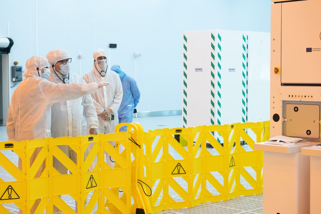
The FAMES Pilot Line installation continues in the brand-new ISO 5 clean room at CEA-Leti, inaugurated at the beginning of this year. The project plans for 71 pieces of equipment on this campus, 30 of which have already been delivered.
A New Era in Wafer-Scale Device Characterization for VTT
We are thrilled to announce a transformative upgrade to VTT’s laboratories: the acquisition of five new state-of-the-art electrical parameter analysers with fast pulsing capabilities. The upgrade is vital to VTT’s goal of developing a wafer-scale pilot-line for back-end-of-line (BEOL) compatible ferroelectric field-effect-transistors (FeFETs).
SAL receives Applied Materials PECVD tool for 200mm dielectrics thin films deposition

Silicon Austria Labs has received its Centura™ PECVD tool from Applied Materials, supporting dielectrics deposition for RF circulators on 200mm wafers. The tool is in commissioning phase and targets the end of 2025 for full qualification.
