
How FD-SOI is 150 more secure than bulk versus Laser Fault Injection?

A publication at IEEE IOLTS conference in July 2026 has highlighted the strong advantage of the FD-SOI CMOS technologies as compared to the legacy bulk ones.
High-Bandwidth CMOS regulated cascode based transimpedance amplifier for short-range Optical communication

Designed in a 22 nm FD-SOI technology and operating from a 0.8 V supply, the Regulated Cascode (RGC) based TransImpedance Amplifier (TIA) achieves a transimpedance gain of 75.5 dBΩ and a −3 dB bandwidth of 4.3 GHz while driving a 150 fF GaN photodiode.
Hybrid hardware advances energy-efficient optimization

By coupling memristors and stochastic magnetic tunnel junctions, the prototype solves hard tasks and could enable compact, low-energy accelerators
Planar self-biased circulators design and simulation
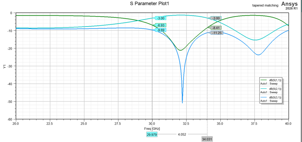
Simulations by SAL show promising performance for planar self-biased circulators, that are much smaller than the existing solutions relying on permanent magnets. This is the first step towards full integration of RF devices on FD-SOI technology.
3D Integrated Power Conversion: Tyndall and CEA-Leti Bring DC-DC Conversion Inside Advanced Packages
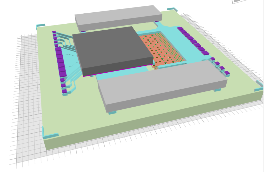
A major milestone in advanced power delivery technologies with the tape-out of a Power Management Integrated Circuit (PMIC) in advanced FD-SOI technology.
Localised Strain Engineering for Next-Gen FD-SOI MOSFETs
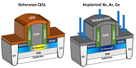
CEA-Leti successfully demonstrates how targeted Xe, Ar, and Ge ion implantations can modulate the mechanical strain of the Contact Etch Stop Layer (CESL).
SADP implementation at the gate-level patterning for the 7nm FD-SOI node
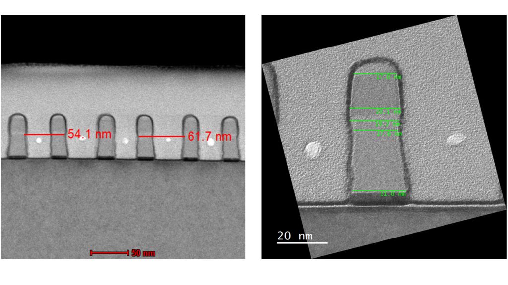
These results demonstrate the feasibility of extending planar FD-SOI technology toward 7nm node using a low-cost gate patterning solution such as SADP.
Ferroelectric HfO2/ZrO2 Superlattice Capacitors with High Center to Edge Wafer-Scale Uniformity
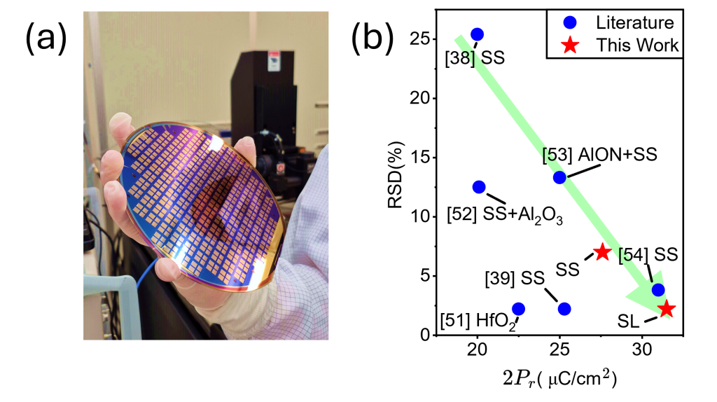
Ferroelectric HfO₂/ZrO₂ superlattice capacitors were fabricated with high wafer-scale uniformity by reducing the impact of process variations.
Impact of Device Position within the Silicon Active Area on Self-Heating and Thermal Coupling in FDSOI Transistors
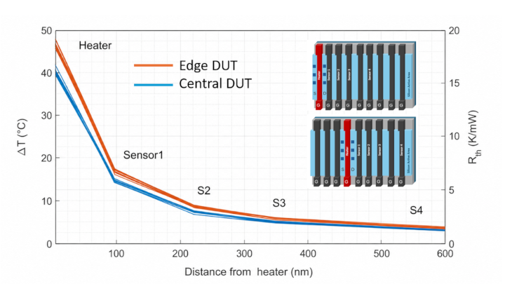
UCLouvain and CEA-Leti analyzed how the transistor position within the silicon active area affects self-heating and thermal coupling in FDSOI Technology.
Release of the first 10 nm FD-SOI technology Pathfinding PDK
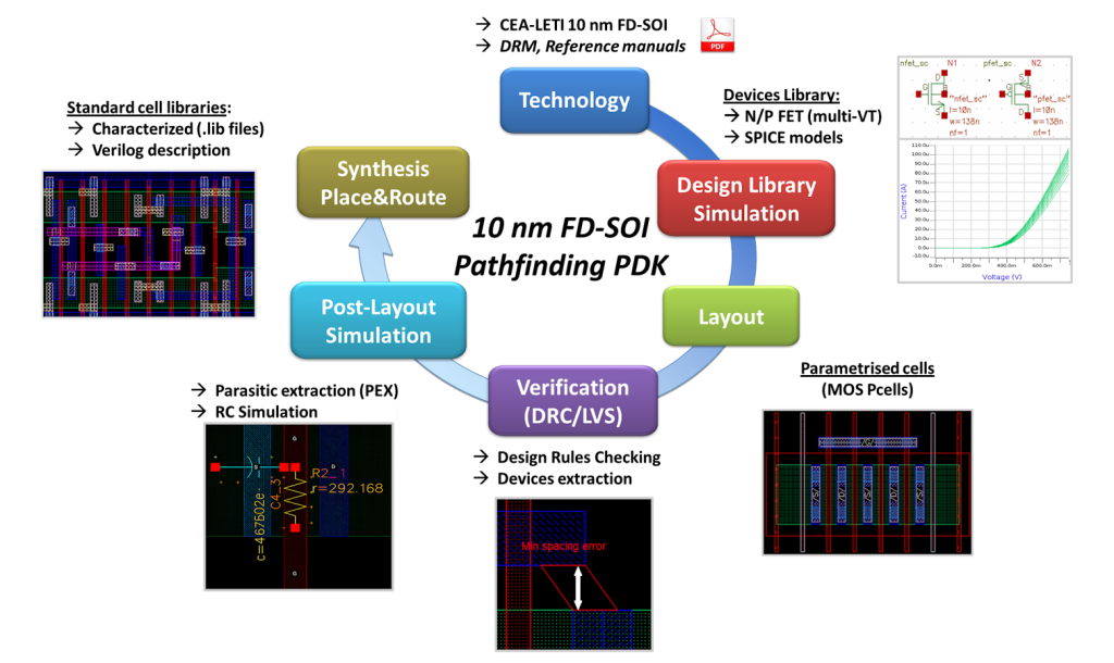
The first Pathfinding Process Design-Kit (PDK) for the 10 nm FD-SOI technology node is now available. This PDK enables an early evaluation of the technology for digital applications.


